
CD4013 circuit
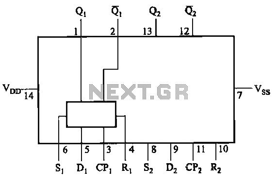
The CD4013 dual D flip-flop is a versatile digital memory circuit used for storing binary information. Each flip-flop has two inputs, D (data) and CLK (clock), and two outputs, Q and Q' (complement of Q). The flip-flop captures the value present at the D input on the rising edge of the CLK signal, transferring this value to the Q output. The Q' output always reflects the inverse of the Q output.
The internal structure of the CD4013 consists of multiple stages of logic gates configured to form the flip-flop functionality. The device operates with a supply voltage range of 3V to 15V, making it suitable for various applications in both low and high voltage environments. The propagation delay between the clock input and the output state change is typically around 50 nanoseconds at a supply voltage of 5V, which makes it suitable for moderate-speed applications.
Pin configuration is critical for proper integration into circuits. The CD4013 has 14 pins, with the primary pins being:
- Pins 1 and 2: D input and CLK input for the first flip-flop.
- Pins 3 and 4: Q output and Q' output for the first flip-flop.
- Pins 5 and 6: D input and CLK input for the second flip-flop.
- Pins 7 and 8: Q output and Q' output for the second flip-flop.
- Pins 11, 12, 13, and 14 are used for power supply and ground connections.
The CD4013 is widely used in digital circuits for applications such as data storage, state machines, and frequency division. Its ability to interface with various logic families enhances its applicability in diverse electronic designs. The interchangeable models (TC4013, MC14013, etc.) offer flexibility in sourcing components while maintaining compatibility with the original design specifications.CD4013 dual D flip-flop on the rising edge. Its internal block diagram and pins are shown. Ministry of standard model C043, GB model CC4013, substitutable or interchangeable models TC4013, MC14013, C073, SG822 and the like.
Related Circuits
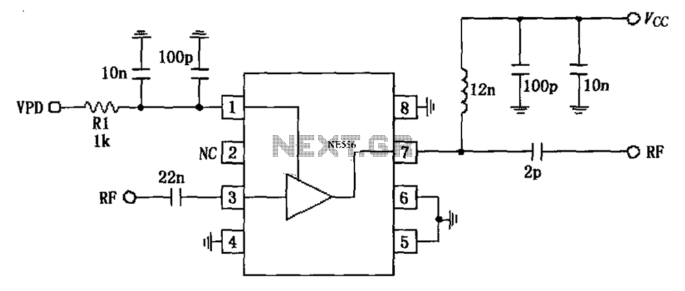
The circuit is based on an 880 MHz RF2347 low noise amplifier application. The radio frequency (RF) signal enters through input pin 3, and after amplification, the output is available at pin 7. The amplifier is directly coupled to...

This picture and schematic were intended for posting on my Watson's blog, but it did not get published. The circuit schematic in question likely includes various electronic components arranged to perform a specific function. Typically, such schematics are used to...
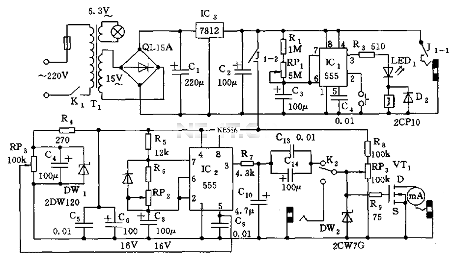
The information apparatus includes a buck rectifier power supply providing Vdd at +12V, a timing circuit, a multivibrator, and the output from the first amplifier. The components R1, RP1, and C3 are used to initiate timing, with the timing...

This circuit is designed as a low dropout charger using a MOSFET as the pass element; however, it does not incorporate current limiting. The circuit diagram illustrates a straightforward design. It utilizes Q3 and a Schottky diode to isolate...
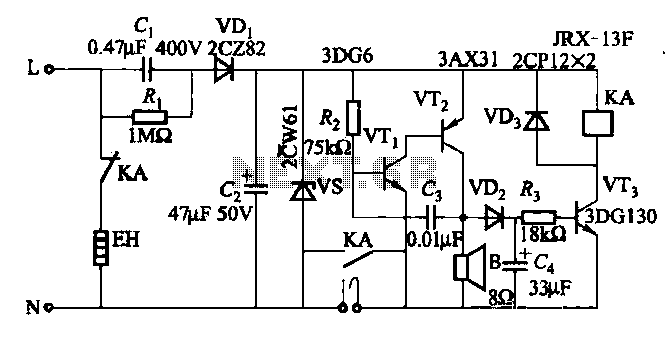
When the water boils, it not only triggers the police but also cuts off the heater power. A temperature sensing element is integrated with a fluorescent neon light bulb, which is restructured within the starter. The described circuit features a...
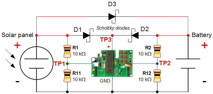
To obtain the power supply graphs on the previous page, the circuit is designed to independently monitor the power sources with the addition of a few resistors. Diode D3 allows the solar panel voltage to charge the batteries, while...