
Cheap And Cheerful Transistor Tester
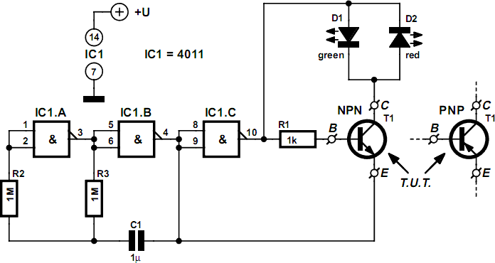
The circuit design leverages the characteristics of the CD4011B quad NAND gate IC, facilitating the implementation of an oscillator and inverter within a compact form factor. The oscillator, formed by the combination of IC1.A, IC1.B, R2, R3, and C1, operates at a frequency that can be adjusted by varying the resistor and capacitor values, allowing for flexibility in the flashing rate of the LEDs. The output from the oscillator at pin 4 is crucial as it provides the necessary signal to determine the operational state of the transistor being tested.
The use of the inverted output from IC1.C is particularly significant, as it allows the circuit to effectively toggle the biasing conditions of the transistor. This toggling is essential for determining the functionality of both NPN and PNP transistors, as it ensures that the device under test experiences both forward and reverse bias conditions, which are critical for accurate testing.
The selection of LEDs D1 and D2 should consider their forward voltage drop and efficiency, as these factors influence the overall performance of the tester. High-efficiency LEDs will ensure that the current flowing through them remains within safe limits while still providing adequate brightness for visual indication.
In terms of power supply considerations, the recommendation to operate within a 3 V to 4.5 V range is based on the need to protect the transistor under test from excessive voltage, which could lead to damage or inaccurate readings. The use of two 1.5 V batteries in series is a practical solution, providing a stable voltage source that is easy to replace.
Overall, this transistor tester circuit is a valuable tool for electronics engineers and hobbyists alike, offering a straightforward method to quickly assess the functionality of transistors in various applications. Its simplicity, combined with effective visual feedback, makes it an essential addition to any electronic testing toolkit.By using a simple visual indicating system, this small transistor tester allows you to run a quick go/non-go` check on NPN as well as PNP transistors. If the device under test is a working NPN then the green LED (D1) will‚ash, while the red counterpart will‚ash for a functional PNP device.
However if the transistor is shorted, both LEDs will ‚ash, and an open-circuit device will cause the LEDs to remain off. The circuit is based on just one CD4011B quad NAND gate IC, four passive parts and two LEDs. The fourth gate in the IC is not used and its inputs should be grounded. Alternatively, you may want to connect its inputs and output in parallel with IC1. C to increase its drive power to the transistor test circuit. IC1. A and IC1. B together with R2, R3 and C1 form an oscillator circuit that generates a low-frequency square wave at pin 4. This signal is applied to the emitter of the transistor under test as well as to inverter IC1. C. The inverted signal from IC1. C and the oscillator output then drive the test circuit (LEDs, device under test, R1) in such a away that the voltage across that part of the circuit is effectively reversed all the time.
For example, with an NPN transistor under test, when pin 10 is High and pin 4, Low, current‚ows through LED D1 and the forward biased transistor. However, no current will‚ow when pins 10 and 4 change states, since the transistor is then reverse-biased.
The green LED, D1, will therefore‚ash at the rate determined by the oscillator. As you would expect to happen, a PNP transistor will be forward biased when pin 10 is Low and 4, High, enabling current to‚ow through the red LED in that case. A supply rail of around 3 V (two series connected 1. 5-V batteries) should be adequate. To prevent damage to the transistor under test, supply voltages higher than 4. 5 V should not be used. Because the LED currents are effectively limited to a few mA by the output of IC1. C (also slightly dependent on the supply voltage), it is recommended to use high-efficiency devices for D1 and D2.
🔗 External reference
Related Circuits
The following circuit illustrates a Mains Remote-Alert Circuit Diagram. Features include simple circuitry, with the transmitted signal being conveyed effectively. The Mains Remote-Alert Circuit is designed to provide a notification system that alerts users about the status of mains power....
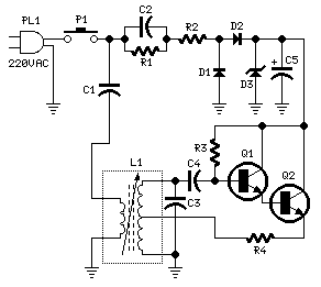
This circuit is a recording signal amplifying transistor circuit that illustrates the functioning of a microphone signal amplifier. After adjustment through potentiometer RP1, the signal is applied to the transistor VT1, which operates as a common emitter amplifier. The...
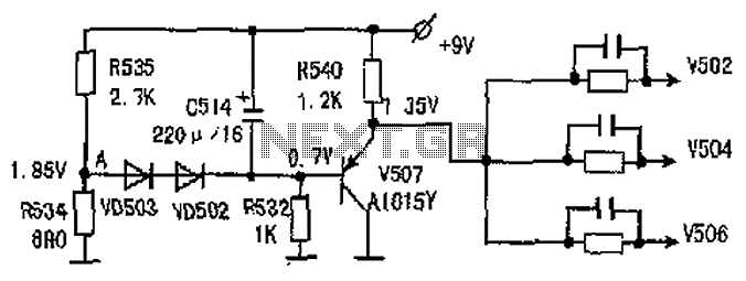
The common-emitter amplifier circuit V502, V504, V506 is designed to generate a static potential bias voltage through an emitter follower configuration, as illustrated in Figure 3. The active filter is formed by components V507, VD502, and VD503. The emitter...

This is an integrated electronic mailbox circuit diagram designed for a front door. It activates when the door is opened. Additionally, when the cabinet photo detector is exposed to light, it will... The integrated electronic mailbox circuit is designed to...
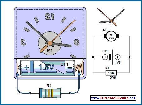
The circuit described is suitable for indicating the capacity of a battery using a low-cost electric clock. By connecting a resistor across the battery terminals, the battery discharges at a faster rate than it would with the clock alone....
This simple circuit is designed to test transistors in a circuit, capable of measuring down to 40 ohms across the collector-base or base-emitter junctions. It is also suitable for checking output power transistors in amplifier circuits. The operation of...