
555 Timer Frequency and Duty Cycle Calculator
The SE555/NE555 timer is a highly versatile integrated circuit widely used in various timing applications, including pulse generation, oscillation, and timers. It operates in two primary modes: monostable and astable. In monostable mode, the timer produces a single output pulse of a specified duration in response to a trigger signal. The duration of the pulse is determined by external resistors and capacitors connected to the timer.
In astable mode, the 555 timer continuously oscillates between high and low states, generating a square wave output. The frequency and duty cycle of the oscillation can be easily adjusted by varying the resistor and capacitor values. This makes the 555 timer ideal for applications such as LED flashers, tone generators, and clock pulses.
The internal architecture of the 555 timer includes two voltage comparators, a flip-flop, a discharge transistor, and a resistor divider network. The voltage comparators compare the input voltage at the trigger and threshold pins with reference voltages derived from the supply voltage. The flip-flop controls the output state based on the comparison results, and the discharge transistor is used to reset the timing capacitor when the output goes low.
For practical applications, the 555 timer can be interfaced with various components, including transistors for driving higher loads, diodes for protecting against back EMF, and capacitors for timing adjustments. The flexibility of the 555 timer allows it to be used in a wide range of electronic projects, from simple LED blinkers to complex timing circuits in industrial applications. The ability to operate over a broad supply voltage range enhances its usability in different environments and applications.First introduced by the Signetics Corporation as the SE555/NE555 about 1971. Pin connections and functions: (See schematic below for basic circuits) Pin 1 (Ground) - The ground (or common) pin is the most-negative supply potential of the device, which is normally connected to circuit common when operated from positive supply voltages. Pin 2 (Trigg er) - This pin is the input which causes the output to go high and begin the timing cycle. Triggering occurs when the trigger input moves from a voltage above 2/3 of the supply voltage to a voltage below 1/3 of the supply. For example using a 12 volt supply, the trigger input voltage must start from above 8 volts and move down to a voltage below 4 volts to begin the timing cycle.
The action is level sensitive and the trigger voltage may move very slowly. To avoid retriggering, the trigger voltage must return to a voltage above 1/3 of the supply before the end of the timing cycle in the monostable mode. Trigger input current is about 0. 5 microamps. Pin 3 (Output) - The output pin of the 555 moves to a high level of 1. 7 volts less than the supply voltage when the timing cycle begins. The output returns to a low level near 0 at the end of the cycle. Maximum current from the output at either low or high levels is approximately 200 mA. Pin 4 (Reset): - A low logic level on this pin resets the timer and returns the ouput to a low state.
It is normally connected to the + supply line if not used. Pin 5 (Control) - This pin allows changing the triggering and threshold voltages by applying an external voltage. When the timer is operating in the astable or oscillating mode, this input could be used to alter or frequency modulate the output.
If not in use, it is recommended installing a small capacitor from pin 5 to ground to avoid possible false or erratic triggering from noise effects. Pin 6 (Threshold) - Pin 6 is used to reset the latch and cause the output to go low. Reset occurs when the voltage on this pin moves from a voltage below 1/3 of the supply to a voltage above 2/3 of the supply.
The action is level sensitive and can move slowly similar to the trigger voltage. Pin 7 (Discharge) - This pin is an open collector output which is in phase with the main output on pin 3 and has similar current sinking capability. Pin 8 (V +) - This is the positive supply voltage terminal of the 555 timer IC. Supply-voltage operating range is +4. 5 volts (minimum) to +16 volts (maximum). The pin connections for the 556 which is a dual 555 timer (2 in one package) are shown in table below.
For example, the two outputs for the two timers of the 556 are on pins 5 and 9 which correspond to the output pin 3 of the 555. 555 556 timer #1 timer #2 - Ground 1 7 7 Trigger 2 6 8 Output 3 5 9 Reset 4 4 10 Control 5 3 11 Threshold 6 2 12 Discharge 7 1 13 + Power Vcc 8 14 14 - The schematics below show the two basic circuits for the 555 timer.
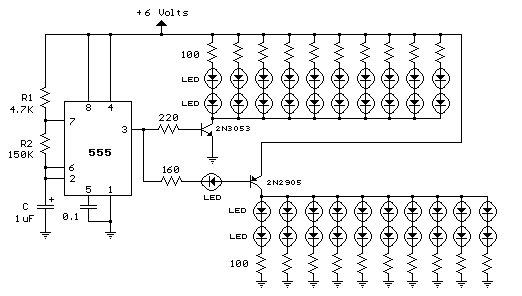
Below is a pictorial view of the 555 timer wired as a LED flasher and powered with a 9 volt battery. The LED will turn on during time T1 and off during time T2. The 555 circuit below is a flashing bicycle light powered with three C or D cells (4. 5 volts). The two flashlight lamps will alternately flash at a approximate 1. 5 second cycle rate. Using a 4. 7K resistor for R1 and a 100K resistor for R2 and a 4. 7uF capacitor, the time intervals for the two lamps are 341 milliseconds (T1, upper lamp) and 326 milliseconds (T2 lower lamp). The lamps are driven by transistors to provide additional current beyond the 200 mA limit of the 555 timer.
A 2N2905 PNP and a 2N3053 NPN could be used for lamps requiring 500 mA or less. For additional current, a TIP29 NPN and TIP30 PNP could be used up to 1 amp. A PR3 is a 4. 5 volt, 500 mA flashlight bulb. Two diodes are placed in series with the PNP transistor base so that the lower lamp turns off when the 555 output goes high during the T1 time interval. The high output level of the 🔗 External reference
Related Circuits
In these applications, a pulse input at a specified percentage is differentiated by a capacitor-resistor (C-R) network. The negative-going edge at pin 6 triggers the input comparator, activating the timer circuit. Similar to a voltage-to-frequency (V-to-F) converter, the average...
The core component of this circuit is the 555 timer IC. The alert sound does not stop immediately when the switch is activated; instead, it ceases automatically after a predetermined time period, which is set by the resistance of...
The monostable 555 timer multivibrator circuit, also known as a one-shot monostable multivibrator, functions as a retriggerable pulse generator. The term "monostable" indicates that the circuit has only one stable state, with the unstable state referred to as the...
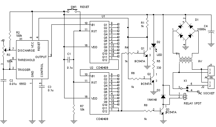
The following schematic diagram is a four-hour timer circuit. Features include ease of construction, a total timing duration of 3 hours and 53 minutes, and a 9V supply voltage. Components utilized in the circuit are a 555 timer IC,...
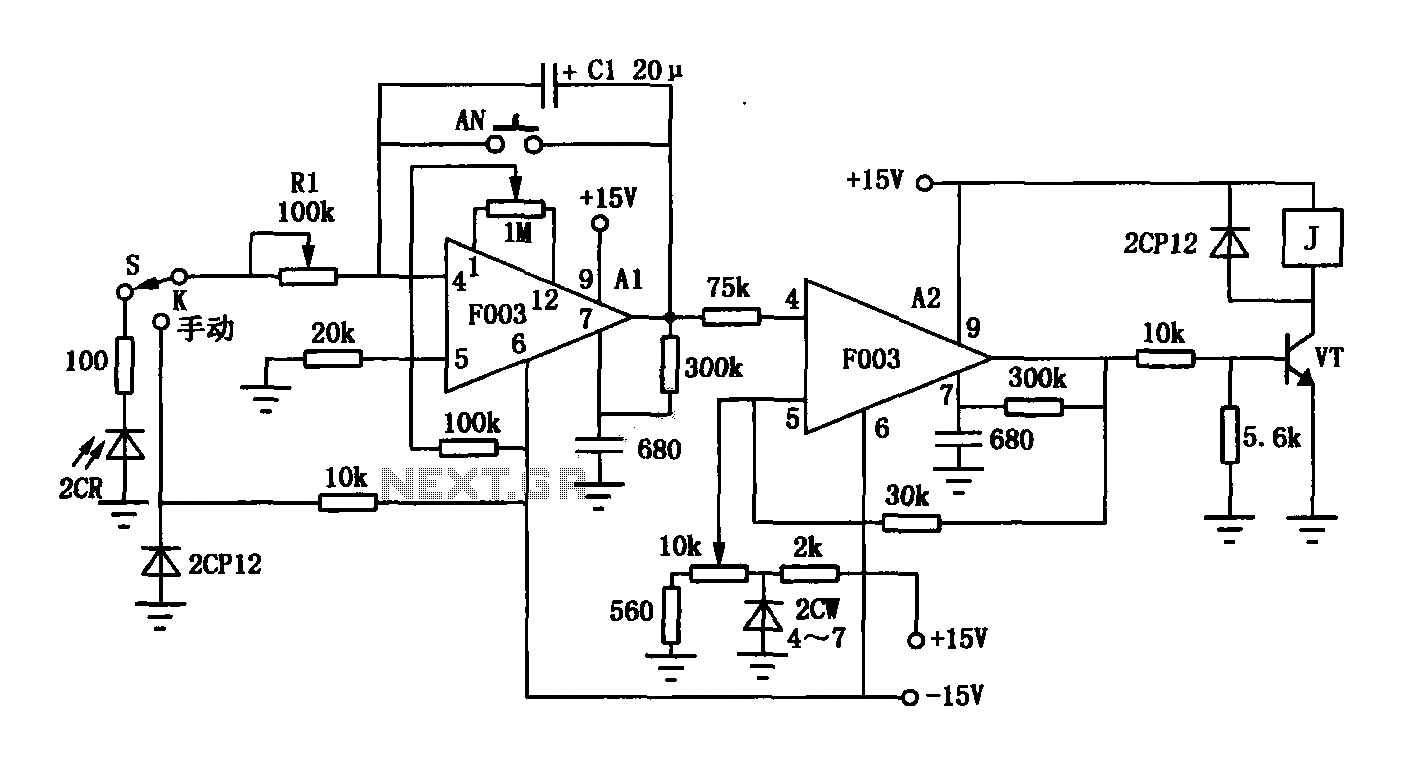
The F003 circuit is a versatile photographic component that functions as an operational amplifier amplifying automatic timer circuit. The operational amplifier A1 serves as an integrator, while operational amplifier A2 is configured as a comparator. A 2CR silicon photocell...
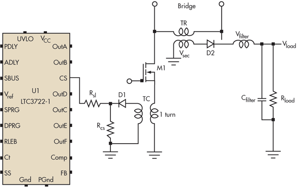
Current-controlled switching-mode power supplies (SMPS) are increasingly popular due to their ability to allow pulse-by-pulse current control and monitoring, enhancing reliability and robustness compared to voltage-controlled alternatives. Current control also removes a positive zero in certain transfer functions, contributing...