

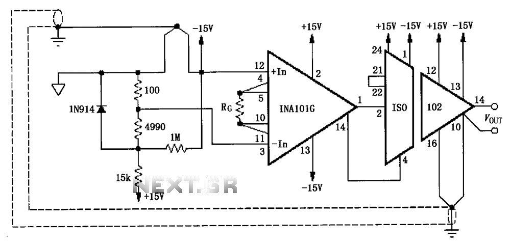

Eliminate loops cold junction compensation amplification circuit ISO102 INA101
As shown in FIG constituted by ISO102 and INA101 have to eliminate ground loops, and high-end off cold junction compensation thermocouple amplifier. This circu...
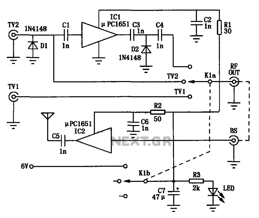
TV signal amplifying circuit diagram conversion
As shown in FIG amplification is used to convert a variety of devices and TV video output signal, such as some VCRs, DVD players need weak output signal amplif...
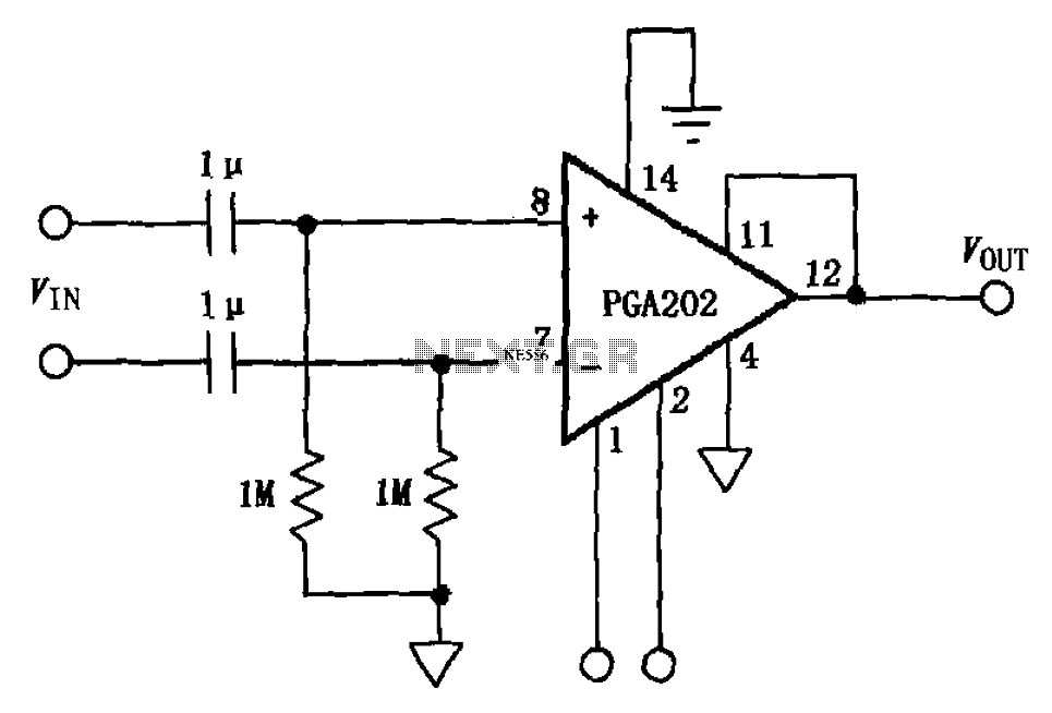
AC-coupled differential amplifier PGA202
As shown in FIG PGA202 constituted by AC-coupled differential amplifier. The circuit at the input PGA202 plus two 1 F capacitors and two 1M resistor compositio...
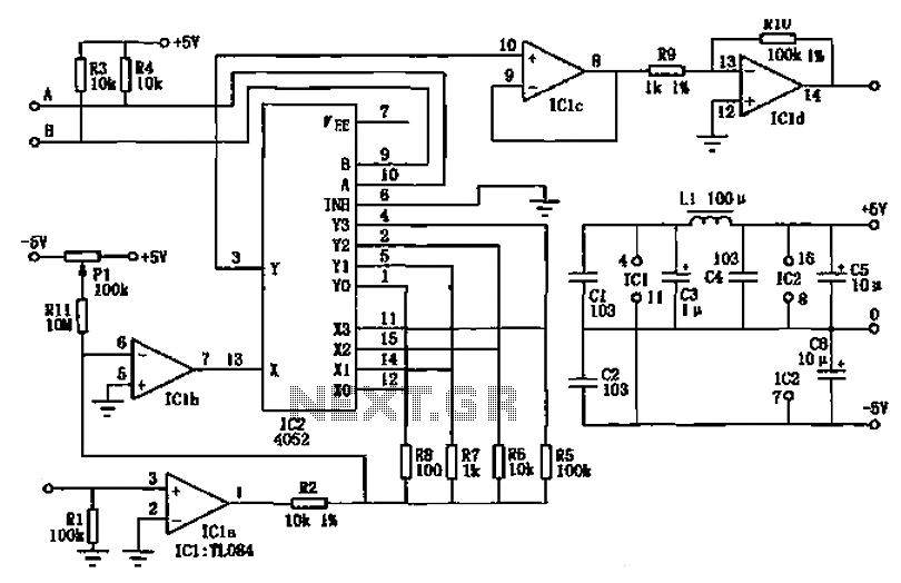
Gain amplifying circuit diagram or programming
As shown in FIG PGA103 constituted by a wide input voltage range of the amplifier. 11.3k with 102k resistor voltage divider circuit dividing ratio of about 1/1...
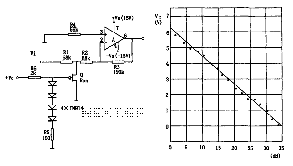
Voltage controlled gain amplifier LM307
As shown for the voltage-controlled gain amplifier. Use FET gate voltage and the drain - source resistance between RSD to approximate logarithmic relationship ...
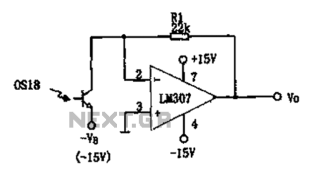
Photoreceiving circuit diagram LM307 amplifier configuration
As shown for the photoelectric receiver amplifier. Photo receiver amplifier for amplifying circuit amplifies the electrical signal photodiode or phototransisto...
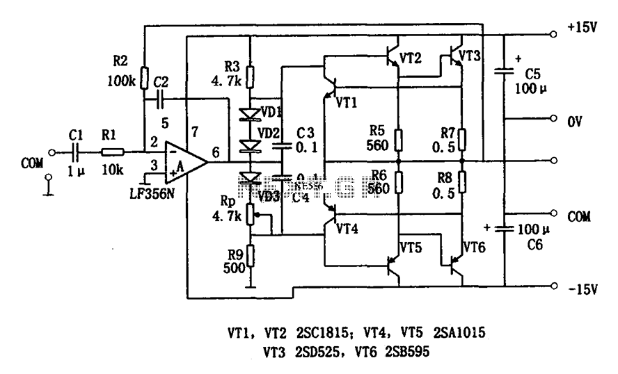
7W Audio Power Amplifier LF356
As shown for the low-frequency output 7W power amplifier circuit. The circuit uses a FET input type operational amplifier LF356 integrated as a voltage amplifi...
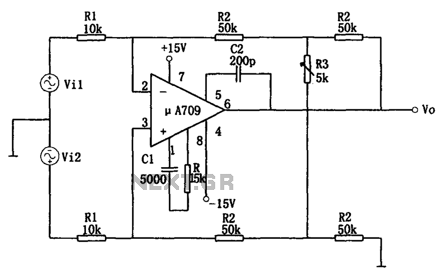
Variable gain differential amplifier circuit diagram A709
As shown for the configuration of the variable gain A709 differential amplifier circuit. The biggest advantage of the circuit is in keeping CMRR KCMR same prem...
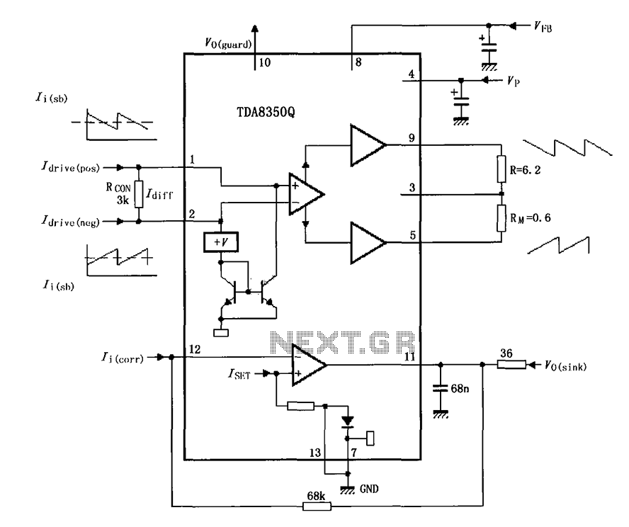
TDA8350Q test circuit diagram
As shown for the TDA8350Q test circuit, the circuit is in the push-pull amplifier output terminal resistor as a dummy load testing alternative deflection coil....
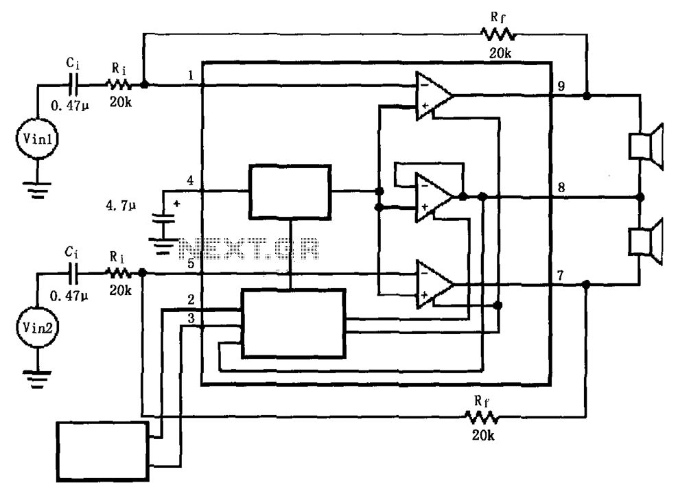
LM4911 without an output capacitor OCL power circuit
As shown for the LM4911 no output capacitor (OCL) power circuit. Without an output capacitor (OCL) power circuit without using squelch control (Mute), because ...
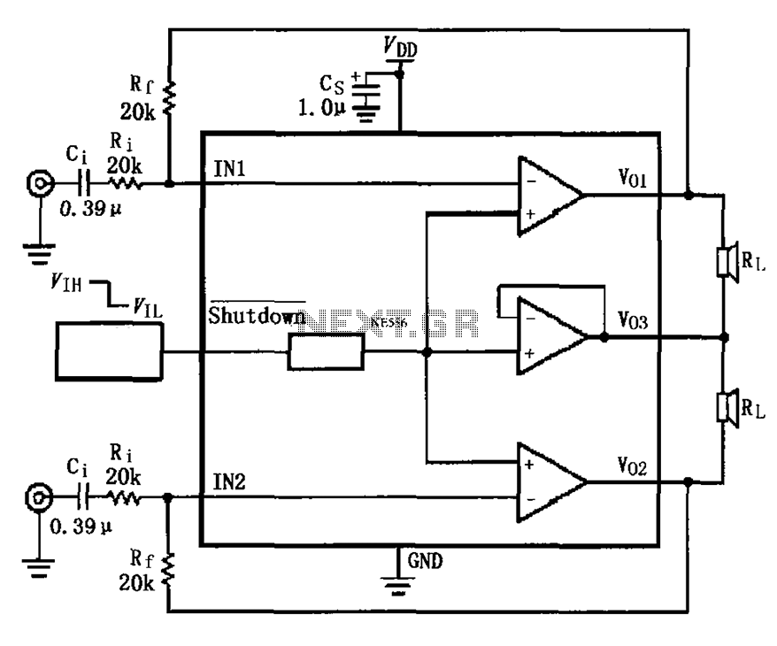
A typical circuit for the LM4910 two-channel amplifier
As shown for the LM4910 typical circuit for two-channel amplifier. Left and right channel audio signals are input LM4910 (MSOP/SO package) 1,2 feet, after an i...
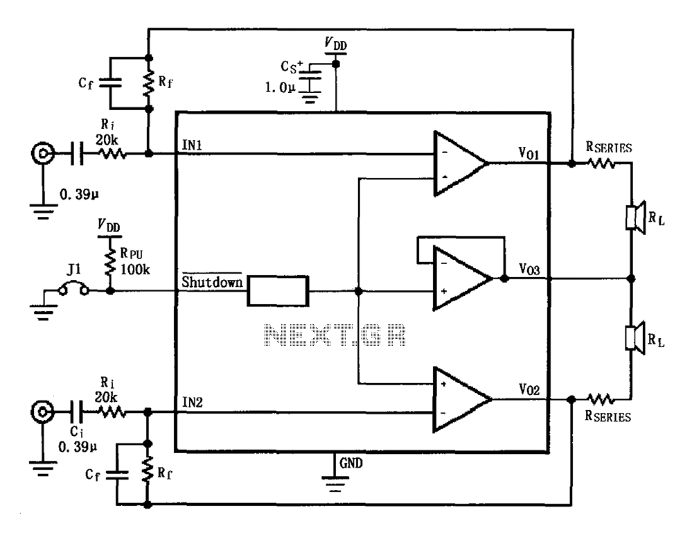
LM4910 minimum output noise reduce the output power circuit
As shown for the LM4910 minimum output noise/reduce the output power circuit. Reduce output noise measures are: between the output terminal of a resistor in se...
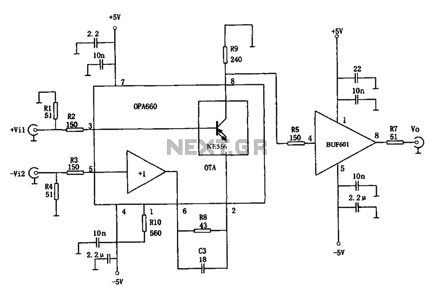
400MHz differential amplifier OPA660 BUF601 schematic
As shown for the 400MHz broadband differential amplifier circuit. The circuit consists of two parts: the incoming broadband differential amplifier integrated c...
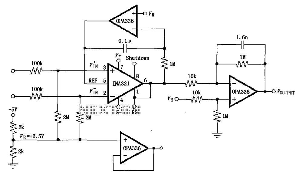
INA321 322 a low-cost medium accuracy ECG machine ECG amplifier
As shown by INA321/322 constitute a low-cost, medium accuracy ECG machine ECG amplifier circuit shown. INA321 input signal from the patients arm around/322, th...
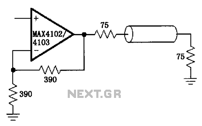
Video by MAX4102 4103 RF distribution amplifier circuit diagram
As shown by FIG MAX4102/4103 Video configuration/RF distribution amplifier. Signal input MAX4102/4103, after amplification the output. To make the transfer pro...
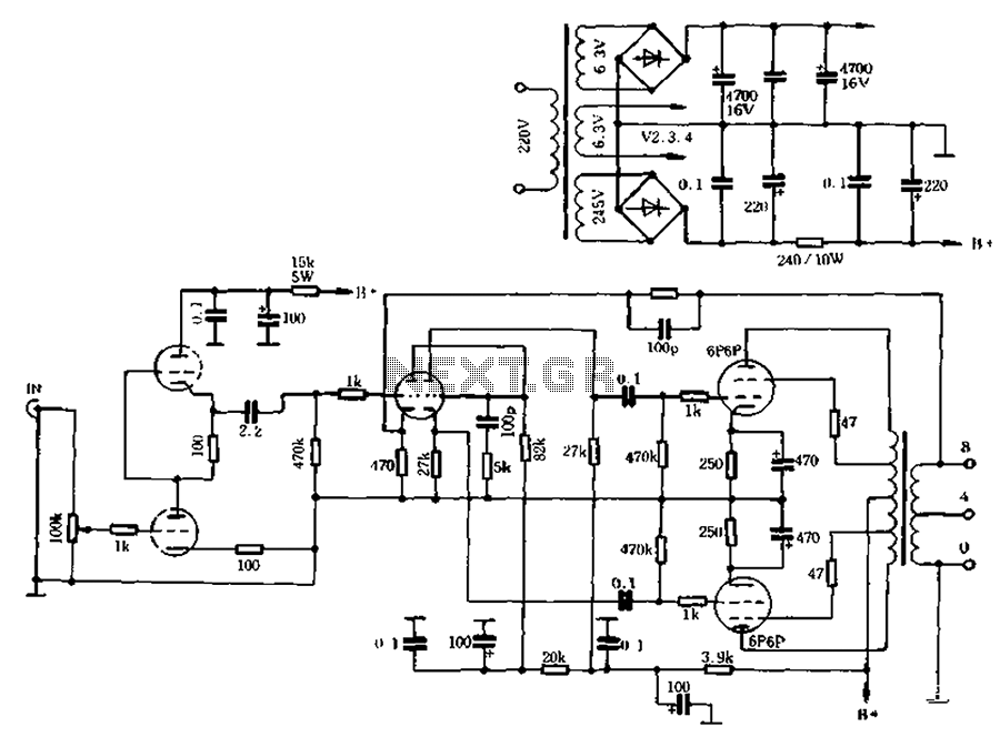
High-quality ultra-linear 10W tube amp
As can be seen from the figure, the self-generated bias amplifier tube for each tube separately to reduce the demanding amateur conditions paired amplifiers cam...
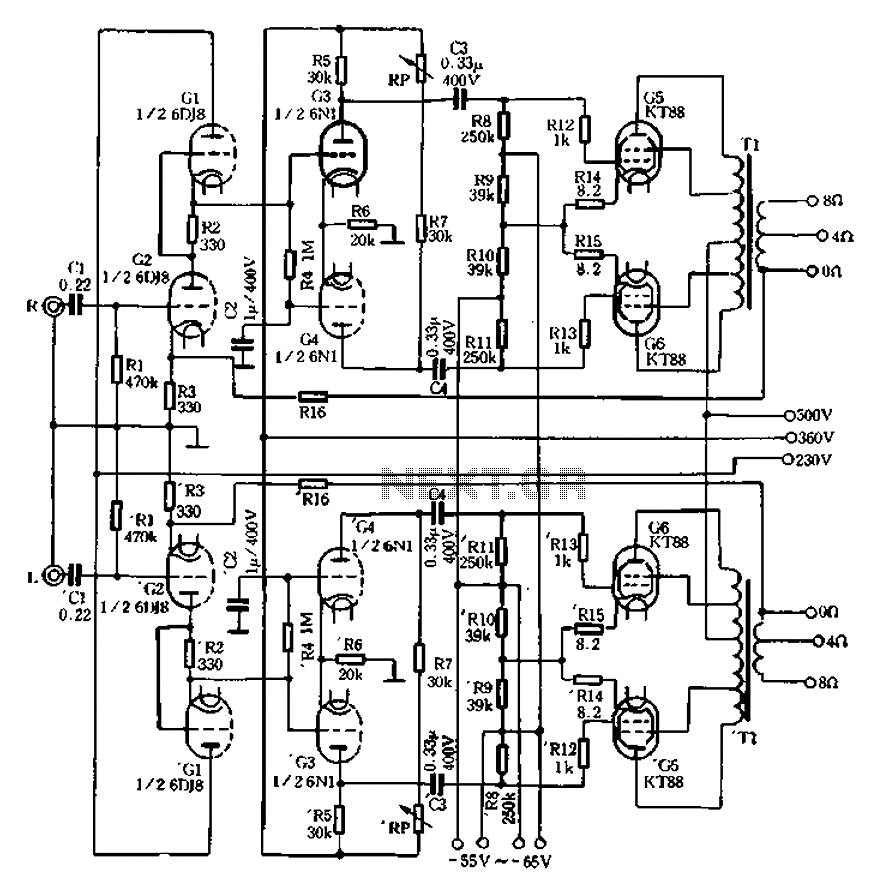
A tube amplifier 01 HI-FI
As a result of high quality materials and advanced technology, the machine output transformer frequency response can reach 10Hz (a 0.8dB) ~ 50Hz (a ldB), to imp...

Application of the differential amplifier circuit OTL amplifier circuit
Application of the differential amplifier circuit OTL amplifier circuit ...
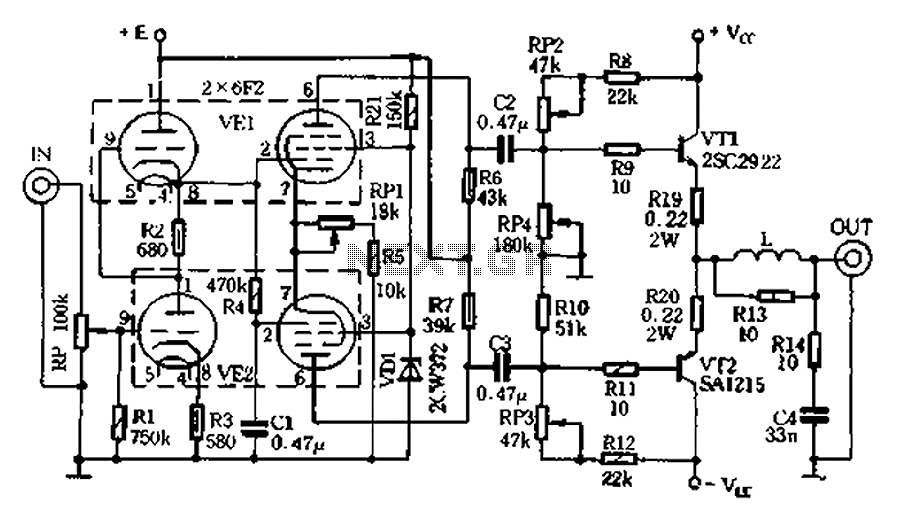
30W Hybrid amplifier 01
And the pre-amplifier stage inverter consisting of two three - 6F2 pentode act, the pins are distributed as shown in Figure 2.9, the electrical parameters such ...
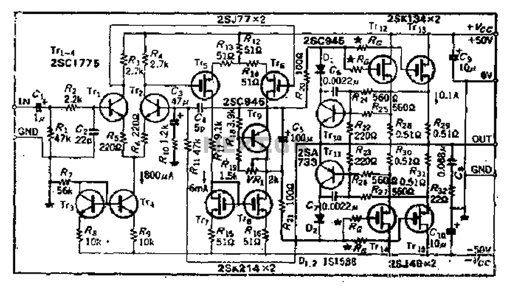
High-frequency characteristics are improved power MOSFET amplifier
And 3 gn same basic circuit, and the second stage is a differential output of the power MOSFET, 2SJ77, a current mirror circuit uses 2SK214. While the operating...