
current mode amp powers 24 ghz
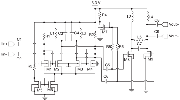
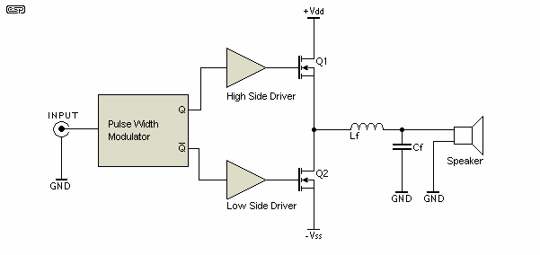
The circuit design for this high-efficiency CMOS power amplifier features a two-stage configuration that optimizes performance for 2.4-GHz applications. The first stage, a differential driver, utilizes current mirrors to ensure precise current amplification while maintaining low power consumption. The driver stage is crucial for preparing the input signal for the subsequent amplification stage, effectively boosting the signal strength without introducing significant distortion.
The second stage employs a current-mode Class D amplifier, which is characterized by its ability to switch the output devices rapidly, thus maximizing efficiency and minimizing heat generation. This stage is designed to operate under zero voltage switching conditions, which significantly reduces switching losses and enhances overall power efficiency. The integration of spiral inductors on the CMOS chip allows for compact design while maintaining the necessary inductive elements for proper operation at high frequencies.
Simulation results indicate that the amplifier achieves a power-added efficiency of 40% at a supply voltage of 3.3 V, with a saturated output power of 0.25 W. These parameters demonstrate the effectiveness of the CMOS technology in achieving high-performance amplification suitable for modern wireless communication applications. The use of a mixed-signal/RF CMOS process further supports the integration of additional RF front-end components, contributing to the development of compact, single-chip solutions for wireless transmitters. The design and simulation methodologies employed ensure that the amplifier meets the rigorous demands of efficiency, output power, and gain, positioning it as a viable option for 2.4-GHz wireless applications.It is possible to apply switch-mode approaches to a silicon CMOS semiconductor process to fabricate a current-mode power amplifier with high gain and efficiency for use in 2. 4-GHz wireless applications. Amplification at 2. 4 GHz is necessary for a number of different wireless applications, and CMOS offers a low-cost and effective process for achieving respectable gain at that frequency.
In support of wireless transmitters at 2. 4 GHz, a 2. 4-GHz CMOS current-mode power amplifier was developed for improved efficiency. It consists of two differential amplifier stages. The first stage is a driver evolved from current mirrors, while the second stage is a current-mode Class D amplifier. All components, including the inductors, are on the CMOS chip. Simulations performed with a commercial computer-aided-engineering (CAE) software package (from Cadence Design Systems ) indicate high power-added efficiency (PAE) of 40% with 0.
25-W saturated output power and high gain when operating at a 3. 3-VDC supply. The rapid growth of wireless devices and services has driven the need for practical solid-state devices, including amplifiers. Many applications are being served by single-chip radios. 1 Many of the RF front-end functions, such as the low-noise amplifier (LNA), frequency mixer, and voltage-controlled oscillator (VCO) serving as the radio`s local oscillator (LO) have been integrated onto a single chip using silicon CMOS processes.
But some of the limitations of CMOS technology ”such as thermal dissipation, power efficiency, and supply voltage ”have prevented the integration of the power amplifier (PA) output stage. 2 Of course, the PA is a key part of a 2. 4-GHz wireless radio, supporting the transmitter section. PA performance can be judged by a number of parameters, including output power, gain, and efficiency, with one of the more important characteristics (especially for extended battery life) being the efficiency.
3 High efficiency can also translate into less heat produced by the output circuitry. A number of different topologies have been applied for RF PAs, differentiated by the operational states of the active devices (transistors). For example, different classes of linear PAs ”including Classes A, B, and C ”refer to the use of a constant power supply in energizing the transistors.
In contrast, switched-mode PAs ” such as Classes D, E, and F ”turn the power supplies on and off. 4 Each of these types of PA have advantages and disadvantages: Linear amplifiers offer good linearity at the expense of efficiency, while switched-mode amplifiers sacrifice linearity for efficiency. Class D switched-mode amplifiers have often been used for low-frequency applications, but less so at higher frequencies.
At the latter frequencies, the parasitic capacitance discharge losses become excessive. But a modified Class D structure, known as a current-mode Class D (CMCD) PA uses zero voltage switching (ZVS) to minimize discharge losses and can work at higher frequencies. 5-8 Most current-mode Class D PAs have been fabricated with gallium arsenide (GaAs) field-effect transistors (FETs)5, 6 or silicon lateral diffused metal-oxide-semiconductor (LDMO) FETs.
7, 8 The use of these technologies prevents fabrication as a silicon CMOS chip. A two-stage amplifier was designed for high efficiency in a silicon CMOS process. The first, driver stage accepts input current signals and converts them to larger driving signals for the following stage. The second stage is basically a PA. Spiral inductors were used to allow the use of on-chip inductors. For analysis, the amplifier design was simulated using the Cadence Spectre ® CAE program for a CHRT 0.
18- m mixed-signal/RF CMOS process. The simulations revealed that this PA design offers higher efficiency and output power than other CMOS PAs working at the same frequency. 9-13 Figure 1 presents the circuit for this high-efficiency CMOS PA. The driver 🔗 External reference
Related Circuits
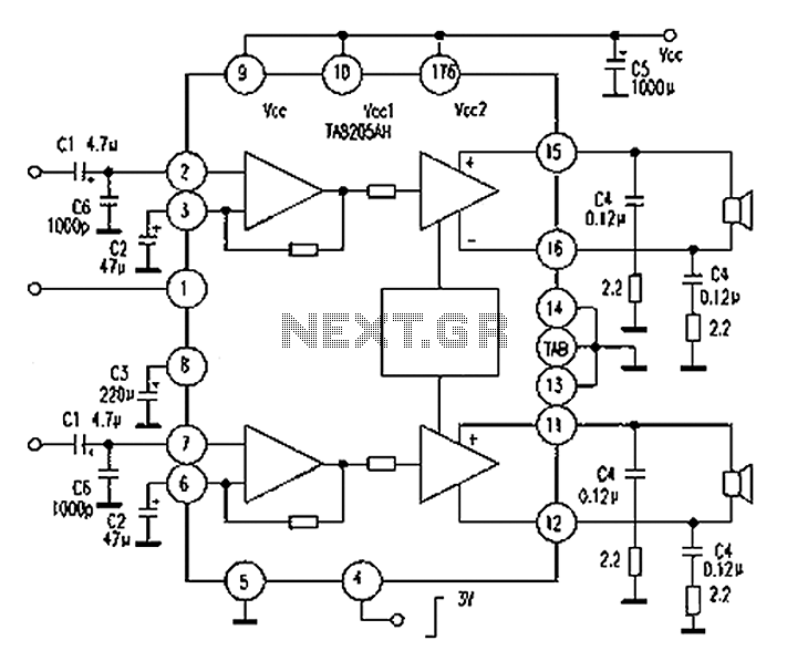
A Mitsubishi Pajero car audio system is experiencing a silent fault, while other features remain operational. The issue is traced to a damaged amplifier IC, specifically the TA8205AH. This integrated circuit, produced by Toshiba, is a dual-channel audio power...
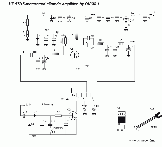
This project and your efforts will provide you with a 0.55...3 watt input to easily 10 watt output. The two linear amplifiers are meant for use with QRP SSB/CW/FM/AM transmitters on the amateur bands 15 and 17 meters can...
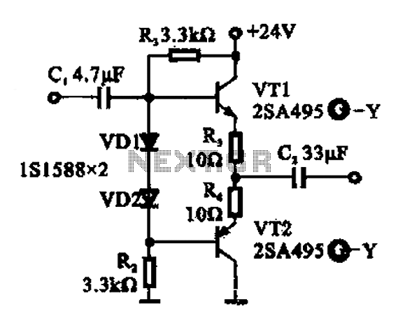
A buffer amplifier is utilized as a transistor emitter follower buffer amplifier for applications that necessitate a high input impedance. The circuit employs a complementary push-pull configuration. The signal input is connected to the base of transistor VT1, which...
One of the critical components is a PWM speed controller, allowing for fine speed adjustments instead of just an "on" mode that runs at full power. This is important for safety. A basic stamp microcontroller was purchased, which includes...
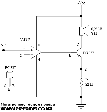
This circuit is one of the simplest voltage-to-current converters designed to drive low loads. In this example, a small 0.25-watt speaker with an 8-ohm resistance is utilized. It is suitable for microcontroller applications or any circuit that employs PWM...
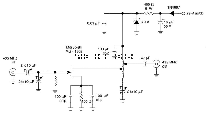
This circuit is a low-noise preamplifier designed for the 435-MHz amateur satellite frequencies. It utilizes a Mitsubishi MGF1302 transistor. A 28-Vdc power source is indicated; however, lower voltages can be employed by adjusting the 400-5-W resistor. The low-noise preamplifier circuit...