
DC to DC Converter
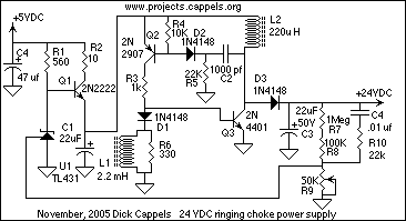
The basic converter provides an output voltage that is about 10 times the input voltage. The voltage boost occurs when the 2N4401 switches off, and the magnetic flux that had been supported by current flowing in the inductor collapses. This rapid change in flux is accompanied by the voltage on the collector of the 2N4401 rapidly rising, limited for the most part by the turnoff time of the transistor, but ultimately being clamped to a diode drop above the voltage across the output capacitor. This type of converter is often referred to as a boost converter or a flyback converter, the latter term referring to the high voltage power supply that was integrated with the horizontal deflection circuits in cathode ray tube television sets. High voltages would be developed when the horizontal scan circuit rapidly made the luminous spot return (or "fly back") to the left side of the screen.
Oscillation frequency is a little under 300 kHz when under load. I had first used a 2N2222 as the NPN because they are pretty common parts, but I could not resist the improved efficiency of the faster switching 2N4401.
After measuring the input voltage required to maintain the output voltage at +24 volts as the load was varied, the basic circuit was then treated as a building block and placed inside an analog regulation loop that could supply the range of voltages needed. From the graph (further below), the analog regulator's output, the emitter of the 2N2222, needs to be able to cover the range from 2.2 volts to about 3.5 volts in order to supply +24 Volts from no load to a 5 milliamp load.
After some refinement to the basic converter, I determined that the converter's analog section should also be able to provide about 40 milliamps to the converter section when supplying a load current of 5 milliamps.
The circuit under discussion is designed to convert a lower voltage into a higher voltage, specifically from a +5 volt input to a +24 volt output. The primary component of the circuit is a boost converter, which utilizes an inductor and a switching transistor (2N4401) to achieve the voltage increase. The operation of the boost converter relies on the principle of inductor energy storage and release. When the transistor is turned on, current flows through the inductor, storing energy in its magnetic field. When the transistor switches off, the magnetic field collapses, inducing a higher voltage across the inductor, which contributes to the output voltage.
The circuit includes a rectifier diode that allows the boosted voltage to charge an output capacitor, smoothing the output voltage. The output voltage regulation is achieved by integrating the converter within an analog regulation loop, ensuring stable voltage output across varying load conditions. The analog regulator is designed to maintain the necessary input voltage to the converter, which is critical for achieving the desired output voltage of +24 volts.
Key considerations in the design include managing switching harmonics and recovery spikes from the rectifier, which could adversely affect the performance of the RF circuit powered by the amplifier. Additional filtering may be employed in subsequent stages to mitigate these issues. The choice of components, particularly the use of the 2N4401 over the 2N2222, reflects a focus on efficiency and performance, with a target oscillation frequency of approximately 300 kHz under load conditions. The design also accommodates a load current of up to 5 milliamps while ensuring that the analog section can provide sufficient current to support the converter's operation.The intended use of the 24 volts is to power an amplifier that will supply wave forms of up to a couple hundred Hz to bias a varactor or pair of varactors in an RF circuit. This meant that the current requirements would be low - probably a little over a milliamp. It also made me worry about recovery spikes from the rectifier, and harmonics from the switching itself, as they might affect the operation of the circuit the power supply is meant to power.
The circuit here only has minimal filtering. Filtering to remove filter glitches will be added to another assembly. I first considered a switched capacitor power supply since this could be made to switch "softly" at a low frequency, but the parts count started looking pretty high considering I had to go from a regulated +5 volt power supply up to a regulated +24 volt output. This would have taken five half wave multiplier stages. The basic converter provides an output voltage that is about 10 times the input voltage. The voltage boost occurs when the 2N4401 switches off, and the magnetic flux that had been supported by current flowing in the inductor, collapses. This rapid change in flux is accompanied by the voltage on the collector of the 2N4401 rapidly rising, limited for the most part by the turnoff time of the transistor, but ultimately being clamped to a diode drop above the voltage across the output capacitor.
This type of converter is often referred to as a boost converter or a flyback converter, the later term referring to the high voltage power supply that was integrated with the horizontal deflection circuits in cathode ray tube television sets. High voltages would be developed when the horizontal scan circuit rapidly made the luminous spot return (or "fly back") to the left side of the screen.
Oscillation frequency is a little under 300 kHz when under load. I had first used a 2N2222 as the NPN because they are pretty common parts, but I could not resist the improved efficiency of the faster switching 2N4401. After measuring the input voltage required to maintain the output voltage at +24 volts as the load was varied, the basic circuit was then treated as a building block and placed inside an analog regulation loop that could supply the range of voltages needed.
From the graph (further below) , the analog regulator's output, the emitter of the 2N2222, needs to be able to cover the range from 2.2 volts to about 3.5 volts in order to supply +24 Volts from no load to a 5 milliamp load. After some refinement to the basic converter, I determined that the converter's analog section should also be able to provide about 40 milliamps to the converter section when supplying a load current of 5 milliamps.
🔗 External reference
Related Circuits
The simplest Analog to Digital Converter (ADC) can be constructed as shown in Figure 1. The input voltage, which can range from zero up to the power supply voltage (Vcc), is converted to a parallel binary code at the...
High-efficiency step-down switching regulators for positive voltages are common; however, negative step-down switching regulators (negative voltage in, negative voltage out, common ground) are less well known, despite their frequent necessity. Setting them up is not particularly challenging, but literature...
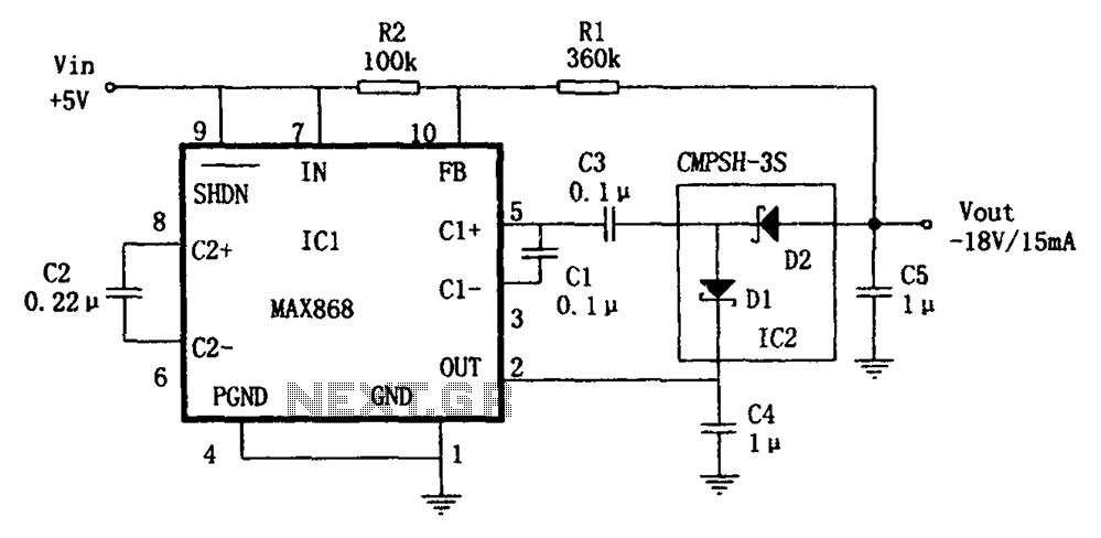
The circuit utilizes the IC1 MAX868 and CMPSH-3S to create a quadruple voltage DC/DC converter power supply. The IC1 MAX868 is an inverting charge pump regulator integrated circuit that can generate an output voltage of up to -2VIN, with...
A DC/DC step-up converter is suitable for use in battery-powered equipment. This converter can be employed to generate supply voltages for internal circuits. The DC/DC step-up converter, also known as a boost converter, is a critical component in various electronic...
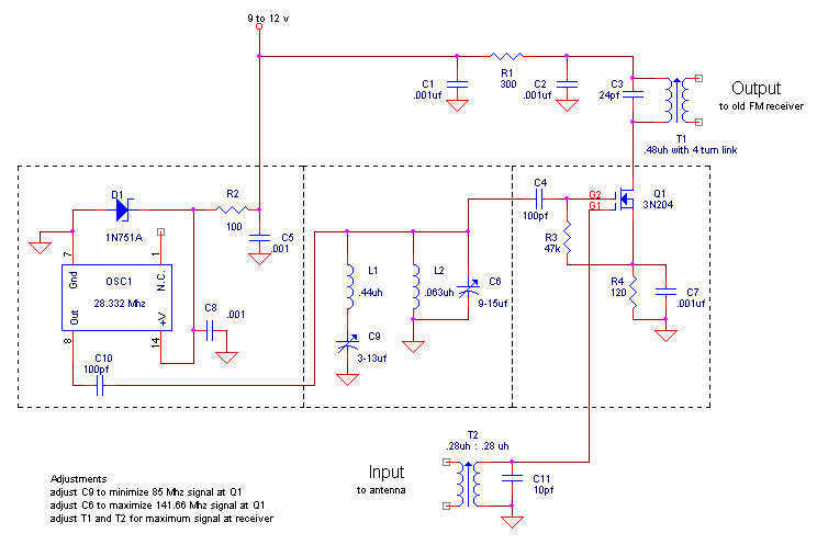
Here is my design for a modern receiving converter for pre-war FM sets. Accordingly, this article presents a design for listening to present day FM stations on a prewar FM set based on a MOSFET transistor and a TTL...
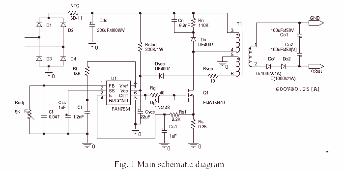
A high voltage step-up DC power supply using adjustable flyback conversion. The described circuit is a high voltage step-up DC power supply that employs an adjustable flyback converter topology. Flyback converters are widely used in applications requiring electrical isolation and...