
Designing 555 Astables
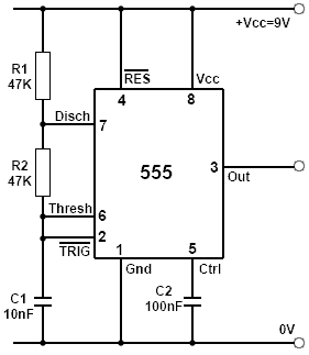
The minimum total resistance value for the combination of R1 and R2 depends largely on the value of R1. The junction of R1/R2 is connected to pin 6 and to the trigger input pin 2. If the value of R1 is less than about 1K ©, there is a danger that the trigger input may not be able reach a low enough voltage to trigger comparator 1, and so oscillations cannot take place.
From this it can be assumed that if R1 must be 1K © or above and R1 + R2 should be kept below 1M ©; a 10nF capacitor would allow a suitable total resistance of around 100K © to be calculated. The basic 555 astable design described above uses two timing resistors when producing square waves. In timing the high (charging) period the timing capacitor (C1 in Fig. 4. 4. 3) is charged via R1 and R2, but only R2 is used whilst discharging C1. In this basic configuration, the resistance used for timing the high period must always be greater than that used during the low period.
The high period of the wave must therefore always be longer than the low period. It follows that the basic version of the 555 astable produces square waves than can be nearly, but never quite 1:1 mark space ratio square waves. The mark to space ratio of a square wave or pulse oscillator is often referred to as the Duty Cycle. This is a more useful term when the purpose of an output wave is to drive some device such as a motor.
It gives a more useful comparison to the power supplied to the motor than describing the mark to space ratio of the output. Changing the duty cycle changes the average DC voltage or DC current level of the output, as shown in Fig.
4. 4. 5 and hence the power supplied to control the speed of the motor. This is also important in driving output devices such as lamps, heaters and many others. The Duty Cycle is a term that describes the percentage of each cycle taken up by the active or high period. For example a square wave with a mark to space ratio of 1:1 has a duty cycle of 50% so the high period takes up 50% of the total period.
In the waveform illustrating negative going pulses in Fig. 7 the duty cycle may be about 80% while in the positive going pulse waveform, the duty cycle may be around 20%. Although the basic form of the 555 astable is limited to producing an output with a duty cycle that is always greater than 50%, one of the great benefits of using the 555 timer as an astable oscillator is the ease with which the circuit can be modified to produce a much wider range of duty cycle.
Where a completely symmetrical output wave (50% duty cycle) is required, an alternative method is to use the circuit shown in Fig. 8. In this configuration, shown using the pin-out of the actual 555 IC, the timing capacitor is still connected to pins 2 and 6 as in the basic astable circuit, but a single timing resistor is now connected to the output, pin 3.
During the high period of the waveform C1 charges from the high output via R1 until the voltage at pin 6 reaches 2/3Vcc and triggers comparator 1. The output now goes low and C1 discharges via R1 until the voltage at pin 2 falls to 1/3Vcc when comparator 2 triggers and starts a new charging period.
As only one resistor is used for charge and discharge in Fig. 4. 4. 6 both charge and discharge times are now identical at 0. 7CR, which gives a simplified formula for the approximate frequency of oscillation. There are however, some drawbacks to this solution for obtaining a 50% duty cycle. Surprisingly the circuit may not always produce a 50% duty cycle. One reason for this is that the design assumes that the output of the 555 changes between 0V and Vcc, but in practice the actual output voltage depends to some extent on the load placed on the output. It is common for example, that in a 555 with a 9V supply the output may change between 0V and just a little over 8V, and with different load resistances, this difference between Vcc and output voltage may again vary.
The trigger points at which the 555 IC switches its output are a fixed proportion of Vcc because they are supplied from the three internal resistors between +Vcc and 0V, but the rate at which the timing capacitor in this design charges now depends, not on Vcc as in the basic design, but on the output voltage. Therefore differences in timing can occur because the voltages at the output pin 3 and at Vcc are not the same, this can affect both the frequency and mark to space ratio.
However performance can be improved in a number of ways to make a number of useful circuits. Pin 5 of the 555 is the Control (Ctrl) pin, which in many applications serves only to decouple the inverting input of comparator 1 inside the IC to prevent noise causing incorrect triggering of the circuit. However, this pin can also function as a useful input, allowing the control of the frequency and duty cycle when the 555 is used in astable mode.
The control input is also connected to the resistor chain in the IC that controls the 2/3 and 1/3Vcc trigger points of the circuit. Therefore by externally applying a DC voltage to pin 5, the internally set trigger points can be altered to lengthen or shorten the charge and discharge periods of the generated wave.
Measuring the voltage on pin 5 would normally show a voltage of 2/3Vcc, and applying a higher voltage than this would increase the time of the charge period as the timing capacitor has to now reach this higher voltage before comparator 1 triggers. Therefore the higher the voltage on pin 5 the longer the charge period and the lower the frequency of the wave.
Reducing the voltage on pin 5 below its normal 2/3Vcc will cause the charge period to shorten and the frequency to increase. Pin 5 therefore provides a method of changing the frequency of oscillation by applying a DC voltage, and since pin 5 can still be effectively decoupled by quite a large value of decoupling capacitor, the potentiometer for controlling the frequency can be located some distance from the oscillator without the problem of introducing noise to the circuit.
Fig. 4. 4. 7 shows how simple control over the duty cycle can be implemented in the basic 555 astable circuit by the use of the control input. A potentiometer VR1 is used to apply a variable voltage to pin 5. The limits of variation is set by R1 and R2 so that the control voltage is not allowed to swing to +Vcc or to 0V, allowing the duty cycle to be adjusted over a range above and below 50%.
One problem with using the control pin in this way is that it affects both the duty cycle and the frequency at the same time. A circuit providing an adjustable duty cycle with a minimal effect on frequency is shown in Fig 4. 4. 8. This is a modified version of the 50% duty cycle circuit shown in Fig. 4. 4. 6. VR1 provides a continually adjustable duty cycle between approximately 35% and 75% avoiding use of the control input therefore allowing adjustment of the duty cycle with little or no effect on the frequency of oscillation.
The two sections of VR1, either side of the slider, added to R1 and R2 effectively provide two separate (and adjustable) values of timing resistor. D1 conducts during the charge period of C1 when the output on pin 3 is high, providing a timing resistance made up of R3, the left hand portion of VR1, and R1.
During the discharge period pin 3 is low, so D1 is reverse biased; D2 now provides a discharge path via R2, the right hand portion of VR1, and R3. The frequency is calculated using the same formula as for the 50% duty cycle circuit shown in Fig. 4. 4. 6, although this will be slightly affected by the forward resistance of the diodes: Also, in this circuit R is now made up of R3 + half of VR1 + R2 (or R1, which is the same value).
Frequencies from a fraction of 1Hz to many tens of kHz can be obtained from Fig 4. 4. 8 by using different combinations of values for the timing capacitor C1 and resistor R3 by a suitable choice of C1. R1 and R2 should be kept equal in value. 🔗 External reference
Related Circuits
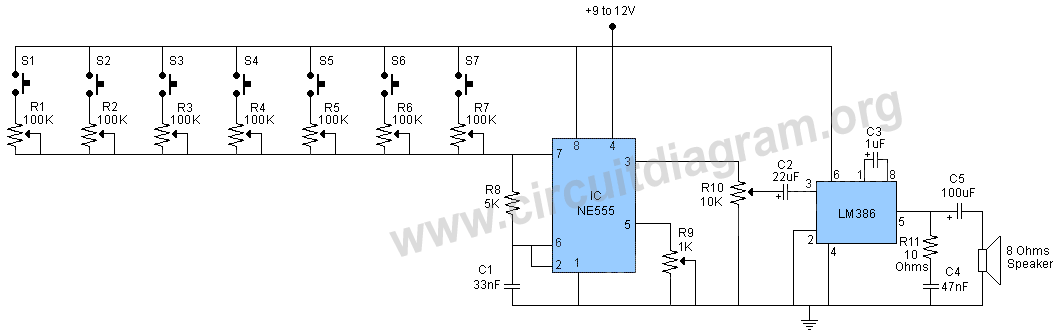
This schematic illustrates a simple 555 organ circuit, which consists of two main components: the 555 timer circuit that generates tones and an LM386 amplifier for driving an 8-ohm speaker. The circuit produces slightly different tones when each switch,...
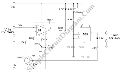
A voltage-to-frequency converter (VFC) circuit is illustrated in the schematic diagram below. The circuit utilizes a 555 integrated circuit (IC) as the central component of its operation. The voltage-to-frequency converter (VFC) is a crucial electronic circuit that converts an input...
This circuit sets the time using a simple model that can accurately maintain the time over extended periods. It employs the CA3140 integrated circuit for its functionality. The circuit utilizes the CA3140 operational amplifier, which is known for its high...
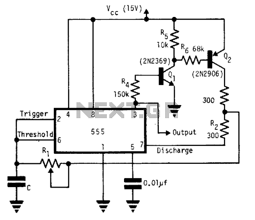
A single timing resistor ensures that the output is a square (50% duty cycle) wave at all frequency settings. Any 555 type of chip will do the job. The circuit utilizes a 555 timer IC configured in astable mode to...
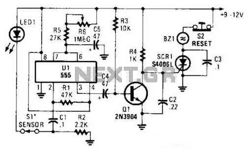
The alarm circuit utilizes a single 555 oscillator/timer (U1) that functions in both the alarm-trigger circuit and the entry-delay circuit. In this configuration, the trigger input of U1 at pin 2 is maintained in a high state through resistor...
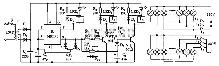
The controller features a buck rectifier circuit utilizing a 555 multivibrator, designed for controlling approximately 220V, 5W low-power parallel lights or 6 to 12V small bulb series. The 555 timer, along with components D3, D4, RP1, and C2, forms...