
Diamond differential amplifier circuit input

The diamond differential input stage of the DC amplifier circuit consists of transistors VTi-VT4. Resistors RP and R6 function as the collector load for VTi, while R sets the electrode load for VT3. Resistors R1, R10, and R11 serve as emitter resistors for VTi to VT4, aiding in establishing a common bias circuit for the DC operating point and providing negative feedback at the same current level. Resistors R2, VD1, R3, R4, and R5 form the DC bias circuit for VTi and VT3. Capacitor C1 is the input signal connected to point A, while C2 and R1 form a low-pass filter with a corner frequency of 60 kHz to limit high-frequency components of the input signal.
Transistors VT5 and VT6, along with their respective bias resistors, comprise the complementary push-pull voltage amplifier stage. Resistors R16, R17, and John form a parallel impedance to constitute the load for VB, VT6, and VT7, while R1 is part of the output bias circuit. Capacitor C4 serves as a high-frequency bypass capacitor, ensuring that higher frequency AC voltage drops close to zero. The complementary push-pull output stage is composed of three Darlington pairs, with NPN transistors VTa, VT10, and VT12, and PNP transistors VT8, VT11, and VT13. VT8 and VT9 utilize a midpoint floating joint, with their bias resistors acting as feedback resistors from the output to the diamond differential midpoint.
The inverting input terminal of the input stage, terminal B, is connected to capacitor C3, which maintains the AC potential at point B close to zero, effectively isolating the large negative feedback loop and allowing only direct negative feedback to flow through the DC feedback loop of the amplifier circuit. This circuit employs a pre-regulated power supply for the front end and a rectified power supply for the output stage, utilizing lower voltage levels for improved performance.Almost all of the DC amplifier circuits are used as the input stage of the differential circuit. Many complementary symmetry circuit also uses a double differential complementa ry sub-circuit and a constant current source with a double differential circuit for the input stage. Because the constant current source has a high dynamic impedance t and common- mode signal has a negative feedback, the circuit has a high stability. However, it is precisely because constant restrictions, when there are significant transient signal at the input, it will cause deterioration of the transient characteristics of the circuit.
Diamond differential circuit by a double differential circuit evolve to, it has the advantage of double differential circuit to overcome its shortcomings, the performance of the circuit is greatly improved. Figure 2-37 is a diamond with a differential circuit for the input stage of the DC amplifier circuit O VTi-VT4 composed of diamond differential input stage, (RP.
Ten R6) is vTI collector load, R is set VT3 the electrode load o R7, heart, Rio, Rl 1 are VTi ~ VT4 emitter resistors, on the one hand and to build a common bias circuit DC operating point of the raised level, but also at the same level of current negative feedback resistor. R2, VDi, R3, R, f matter, R is the DC bias circuit VTi.VT3 o R12, f hair, R13, R14, f) 4, Ris constitute straight VT2, VT4 the flow bias circuit.
Cl input signal is input to the A point. C2, Ri the input resistor, capacitor form a corner frequency of 60kHz low-pass filter to limit the high frequency component of the input signal. VTs, VT6 and their bias resistors complementary push-pull voltage amplifier stage, R16, Rl7 and John into the post-stage impedance in parallel constitute VB, VT6 load o VT7 and Ri constitutes the output of the bias circuit .C4 high frequency bypass capacitance, higher frequency of the AC voltage drop Vm is also close to 00 complementary push-pull output stage uses a power output stage by the three .VTa Darlington composed, VTio.VT12 composition Darling NPN transistor Dayton tube, VTg, VTiI, VT13 composition PNP tube o VT8 associated with VTg using the midpoint of floating joints, to their bias resistor is the feedback resistor from the output to the diamond differential midpoint E the inverting input terminal of the input stage B constituting the DC feedback loop, while the terminal B connected to one capacitor C3, the potential of the point B of the AC zero, thereby cutting off the exchange of large negative feedback loop of the loop, and only become direct flow of negative feedback no AC DC negative feedback amplifier circuit.
this circuit uses the power supply before and after class, respectively, pre-regulated power supply, power supply rectifier output stage after the power supply, and the use of lower voltage o
Related Circuits

Intercom walkie-talkies represent an advanced application of crystal oscillators for voice transmission. Utilizing a crystal-locked oscillator for voice transmission is complex due to the oscillator's fixed frequency, which is challenging to modulate. The primary method for achieving this involves...

It was observed that balls were becoming lodged in the ball trough, failing to load into an upkicker or not resting correctly on the trough ball microswitches or optos, which caused the machine to register a missing ball. Initially,...
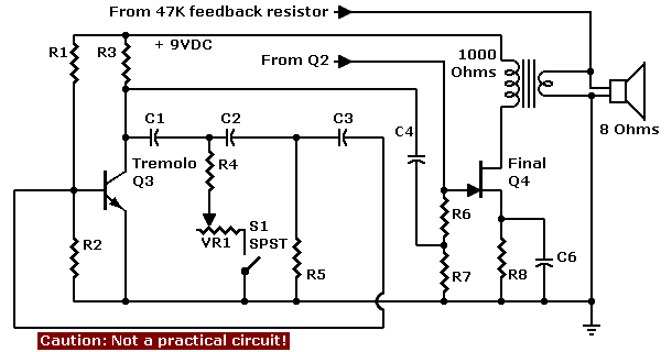
The circuit described is a single JFET design that provides limited gain. By incorporating a source resistor bypass capacitor, the gain can be significantly enhanced, resembling a single stage of the original tube preamp used in guitar amplifiers. It...
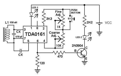
These metal detector circuit diagram is based on the TDA0161 monolithic integrated circuit, designed for metallic body detection by detecting the variations in high frequency Eddy current losses. For detecting metals, TDA0161 require an external LC tuned circuit. Output signal...
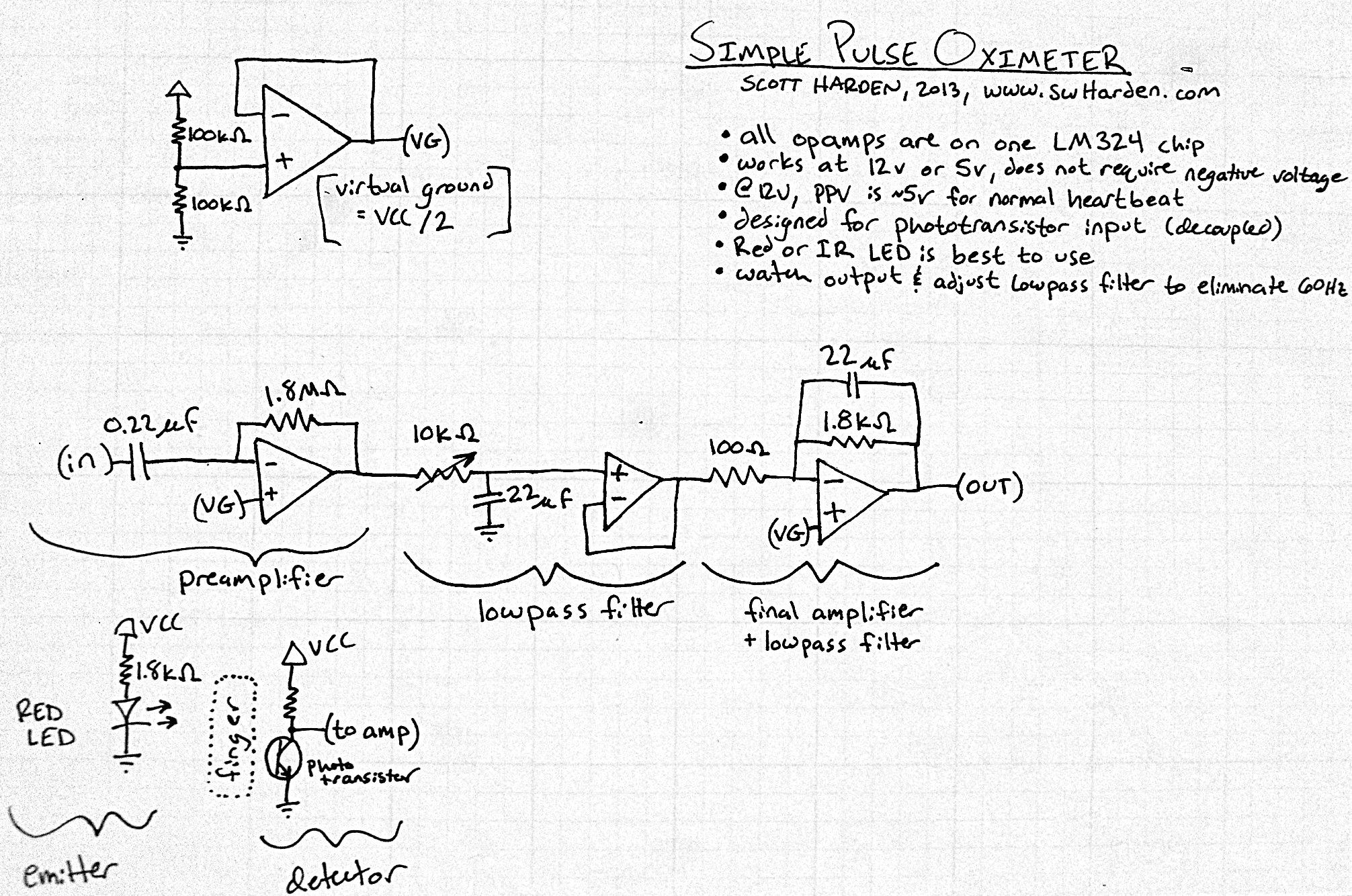
The input capacitor for the phototransistor at the bottom is responsible for feeding the operational amplifier (op-amp). However, the output from the phototransistor consistently remains between ground (GND) and the supply voltage (Vcc). The necessity for an input capacitor...
Before applying power, check for shorts on the board. This design operates from a 5V supply; connecting it directly to a 12V supply will certainly damage it. The current draw is minimal, approximately 70mA, so if using a 12V...