
digital logic purpose of diode in this 555 timer application
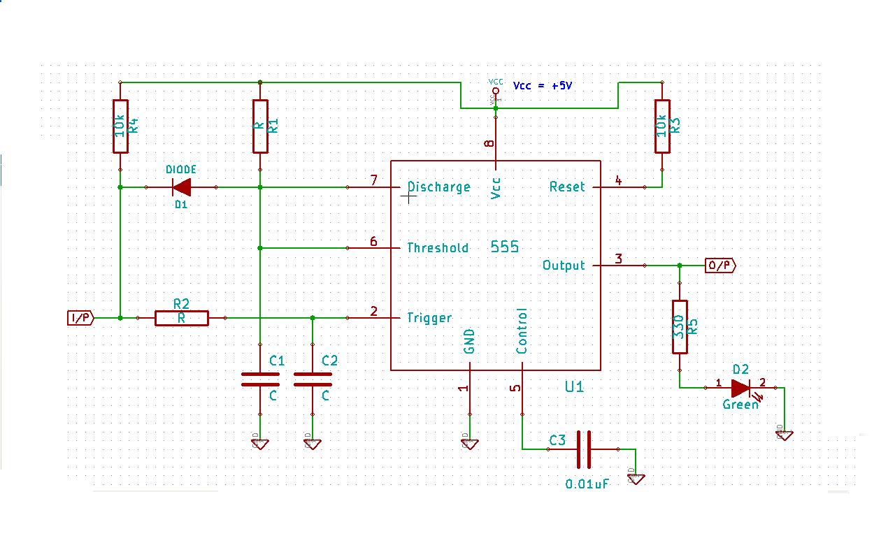
The 555 timer circuit described operates in a monostable configuration, leveraging the timer's ability to produce a single output pulse in response to a trigger signal on the input pin. The design ensures that the output pin (pin 3) remains low at power-up due to the inherent characteristics of the 555 timer and the connection of pin 4 to ground, which disables any unintended triggering.
For the circuit to function as intended, it is essential to select appropriate resistor and capacitor values. Resistor R1 and capacitor C1 form an RC timing circuit that dictates the duration for which the output remains high. The relationship R1 x C1 must exceed the desired pulse duration to ensure reliable operation. Capacitor C2 and resistor R2 are used to set the timing for the input signal; their values must be chosen carefully to meet the specified condition of R2 x C2 < R1 x C1 to avoid unintended behavior.
Regarding the choice of capacitors, electrolytic capacitors are often recommended for C1 and C2 in timing applications due to their higher capacitance values and voltage ratings. While ceramic capacitors can be used, their lower capacitance values may affect the timing characteristics of the circuit. The use of electrolytic capacitors may also provide better stability and reliability in the timing circuit, especially when dealing with longer durations.
The configuration of the flip-flop within the circuit allows for the output to remain latched high as long as the input condition is met. The diode D1 plays a critical role in controlling the discharge path of C1, ensuring that the timing sequence operates as intended. If the threshold pin is left unconnected, it could lead to unpredictable behavior, as the threshold level would not be properly defined, potentially causing the output to not behave as expected.
In summary, careful consideration of component values and configurations is necessary to achieve the desired timing characteristics and ensure reliable operation of the 555 timer-based circuit. The proper selection of resistors and capacitors, alongside the correct wiring of the flip-flop and diode, will facilitate the intended functionality of the circuit.Make a 555 timer base circuit such that O/P pin of 555 is held LOW by default at power on, and the I/P pin is held initially at HIGH at power on. The main requirement of my circuit is that until I/P pin is held LOW for say 200ms, then only the O/P pin must go HIGH and must remain HIGH as long as I/P pin is held LOW.
What will happen if I pull up the control pin to Vcc by say a 1k resistor and remove the capacitor C3 Is the functionality of this circuit affected in some way then I don`t remember where but I definitely saw such a circuit which have this pull-up resistor. What if I keep Threshold pin left unconnected and rest all is same in this circuit - ie anode of diode D1 is now connected only to Discharge pin, R1, C1 and not to Threshold pin!
Will now the circuit work to fulfill my purpose Is the condition R2xC2 < R1xC1 need to be hold true here This is in reference to this question actually. Any suggestions for values of R2, C2, R1, C1, and R4 On some tutorials it was specifically mention to use electrolytic capacitors for C1 and C2 here in schematic even for 1uF values (though they did not say that you must use electrolytic caps but they had drawn schematic with electrolytic caps.
). Is it necessary Will it make any difference Why can`t we use ceramic capacitors here for C1 and C2 I mean to say that what things I need to consider so that this circuit functions reliably and accurately. Absolute accuracy is not required - a tolerance of few tens of ms will work. Whether I should choose higher capacitance for C2 and lower resistance for R2, or higher resistance for R2 and lower capacitance for C2, for 0.
4 x R2 x C2 to be = 1 second typical and 880ms minimum Well, I thought that this update will be better to put as an answer rather that as an edit/update to Question. Also it would take too much space in Question. So I`m putting it here. In this functional block diagram, note that in effect, o/p Q of Flip-flop(FF) is directly connected to pin#3, and o/p Q# of FF is directly connected to base of BJT.
From the description of Working of 555 in monostable configuration, it seems to me that the S-R flip-flop(FF) is implemented as a NOR gate FF in functionality. Assume that the pin#3 is LOW at this point. (Pin#3 can be forced to LOW at power on by driving pin#4 to LOW. pin#4 when LOW causes the o/p Q of FF to be LOW and hence o/p pin#3 is latched at LOW. ) As soon as Pin#2 becomes LOW(< 1/3 x Vcc precisely), V- < V+ for Comp#2 and hence o/p of Comp#2 becomes HIGH.
This makes `S` i/p of Flip-flop(FF) HIGH, and hence we got S = 1(HIGH) and R = 0(LOW) condition at FF inputs. This o/p is latched by o/p stage and thus pin#3 becomes HIGH. At this point since Q# o/p of FF is LOW(Q = HIGH) so, the BJT is in cut-off region and hence high-side of C1 is now not at 0V.
Thus C1 starts charging via R1. During all this time, the Q output of FF will remain HIGH due to the latch of o/p stage of the FF, however the output of the Comp#2 will have become LOW as the V- will have become more positive(due to completion of pulse duration, pin#2 is returning to HIGH) than the V+ input of the comparator. Thus at this point, V- > V+ for Comp#2. => o/p of Comp#2 is LOW. => S = LOW. But since R = LOW too(V+ < V- as voltage across C1 has not yet reached at 2/3 of Vcc - see below), so o/p of the FF stays in its previous state ie Q = 1(HIGH).
This assumption can be guaranteed by choosing C1 and R1 values properly. I`m assuming here that values of C1 and R1 are chosen such that 1. 1 x R1 x C1 > pulse duration. Perhaps of course, pulse duration must be known in advance, as is the case here. Since as soon as pin#6 comes at 2/3 of Vcc, the discharging of C1 begins, we must somehow prevent reaching pin#6 to 2/3 x Vcc, for that duration for which we require the o/p pin#3 to remain HIGH. If we make pin#2 to HIGH, then D1 will again be rever 🔗 External reference
Related Circuits
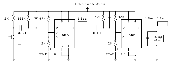
The circuit below demonstrates the generation of a single positive pulse that is delayed in relation to the trigger input time. It is similar to a previously described circuit but utilizes two stages, allowing for control over both the...
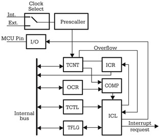
Although there are significant variations between different implementations of the general-purpose timer in various microcontrollers, many similarities exist in the principles of operation and the structure of the timer subsystem. The central element of the timer subsystem is a...
An Analog-to-Digital Converter (ADC) is a circuit integrated into a single chip designed to convert analog signals into digital signals. Typically, an 8-bit ADC chip converts an analog signal ranging from 0 to 5 volts into a digital level...
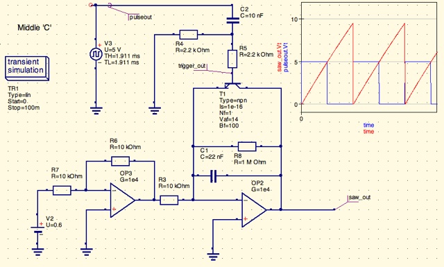
A design for a digitally controlled analog oscillator is being developed. The control voltage is generated by a microcontroller (Arduino) and is utilized through two operational amplifiers, along with a resistor and capacitor network that forms an integrator circuit....

This is a circuit design for a digital voltmeter with an LED display. It is suitable for measuring the output voltage of a DC power supply. The circuit features a 3.5-digit LED display with a negative voltage indicator and...
Two ICM7555 CMOS 555 timers are available, and there is an inquiry about effective AM radio transmitter circuits that utilize one or both of these timers. The ICM7555 is a low-power CMOS version of the classic 555 timer, which can...
Warning: include(partials/cookie-banner.php): Failed to open stream: Permission denied in /var/www/html/nextgr/view-circuit.php on line 713
Warning: include(): Failed opening 'partials/cookie-banner.php' for inclusion (include_path='.:/usr/share/php') in /var/www/html/nextgr/view-circuit.php on line 713