
Extend Timer Range For The 555

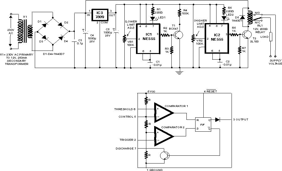
The described circuit leverages the characteristics of the 555 timer in astable mode, enhanced by the use of a pulsed DC voltage to extend the timing interval. The core functionality relies on the switching behavior of transistor T1, which acts as a signal modulator. When the circuit is powered, the bridge rectifier converts AC voltage to DC, producing a pulsed output that fluctuates between high and low states. This pulsed output is fed into the base of T1, causing it to switch on and off at a frequency of 100 Hz.
As T1 conducts, the positive half of the square wave allows current to flow, charging the timing capacitor C1 through the series connection of diode D2 and potentiometer P1. The use of a potentiometer allows fine-tuning of the charging current, which directly influences the timing interval. The choice of a capacitor with a value between 100 µF and 200 µF is critical, as it balances the need for a longer timing period against the effects of leakage currents.
Diode D2 plays a crucial role in maintaining the charge on C1 by blocking reverse current when T1 turns off. This prevents the capacitor from discharging through T1, thereby ensuring that the timing period is determined solely by the charge and discharge cycles of C1. The initiation of the timing sequence is controlled by the push-button switch S1, which, when pressed, allows the circuit to start timing.
Overall, this circuit design provides an innovative solution for applications requiring extended timing intervals while maintaining simplicity and cost-effectiveness. The combination of a 555 timer with a pulsed charging mechanism significantly enhances the capabilities of traditional timer circuits.Anyone who has designed circuits using the 555 timer chip will, at some time have wished that it could be programmed for longer timing periods. Timing periods greater than a few minutes are difficult to achieve because component leakage currents in large timing capacitors become significant.
There is however no reason to opt for a purely digital s olution just yet. The circuit shown here uses a 555 timer in the design but nevertheless achieves a timing interval of up to an hour! The trick here is to feed the timing capacitor not with a constant voltage but with a pulsed dc voltage.
The pulses are derived from the un smoothed low voltage output of the power supply bridge rectifier. The power supply output is not referenced to earth potential and the pulsing full wave rectified signal is fed to the base of T1 via resistor R1. A 100-Hz square wave signal is produced on the collector of T1 as the transistor switches. The positive half of this waveform charges up the timing capacitor C1 via D2 and P1. Diode D2 prevents the charge on C1 from discharging through T1 when the square wave signal goes low. Push-button S1 is used to start the timing period. This method of charging uses relatively low component values for P1 (2. 2 M) and C1 (100 to 200 µF) but achieves timing periods of up to an hour which is much longer than a standard 555 circuit configuration.
🔗 External reference
Related Circuits
This over/under voltage cut-out will save your costly electrical and electronic appliances from the adverse effects of very high and very low mains voltages. The circuit features auto reset and utilises easily available components. It makes use of the...
The timer with a musical alarm is an electronic timer project utilizing the CD4060 integrated circuit. It provides a delay ranging from 1 minute to 2 hours. The circuit diagram for the timer with a musical alarm is part...
This simple LED driver circuit allows the operation of up to seven LEDs using a single NiMH (Nickel Metal Hydride) AA cell. The circuit generates voltage pulses. The LED driver circuit is designed to efficiently power multiple LEDs while maintaining...
The super dimmer is an improved version compared to the standard dimmer currently in use. Testing its performance will provide a clearer understanding of its advantages. The super dimmer operates using advanced technology that allows for finer control over...
This LED circuit replicates the initial LED sequence currently utilized by FISA for Formula One racing. It can also be employed with slot car sets, such as HO scale AFX, Life Like, or Tyco sets, or used in communication-controlled...
Manufacturers of cordless drills typically recommend a battery charging time of three hours. After this time, the battery should be disconnected from the charger to prevent the risk of overcharging. The following circuit is designed to prevent this scenario...