
free heater circuit by Rosemary Ainslie

PS = the Power Supply. This is the Primary Supply of energy to the circuit. Any NEW ENERGY required to run the circuit must come from here. It can be a battery, or any source of DC current. RL = the heating element (load) that has the electrical characteristics of both resistance and inductance. Electrically, the component is operated as an INDUCTOR to be charged and discharged in sequence. C = a Capacitor of sufficient capacitance to act as a secondary power supply to power the circuit and to act as a reservoir to receive the energy returned by the inductive collapse of RL. D1 = a Diode to make sure that energy can only move in one direction, in this case, FROM the power supply TO the capacitor. This component prevents any of the energy returning from the inductive collapse from traveling all the way back to the primary power supply. So, in operation, this Diode will allow the Capacitor C to rise to a voltage that is higher than PS, but it will never allow C to drop to a voltage below PS. SHUNT1 = a low value, calibrated resistor used to measure the currents leaving the Power Supply PS. Current pulses measured here, times the voltage of PS, represent ALL of the energy the circuit is dissipating. Q1 = a Power MOSFET, or any appropriate switching device to allow currents to magnetize the inductive load RL. This includes all of the timing circuitry for the circuit's proper function. D2 = a Diode to complement Q1, to allow currents from C to energize the load RL. D3 + D4 = Diodes to direct the energy of the inductive collapse of RL back to Capacitor C so this energy may be re-used. SHUNT2 = a low value, calibrated resistor used to measure the currents supplied from C (through Q1 and D2) to the load RL. Current pulses measured here, times the voltage of the Capacitor C, represent ALL of the energy supplied to the load RL.
The circuit is designed to operate in the following manner. Q1 is timed to produce current pulses which magnetize RL and then shut off, based on the inductive "current rise-time" of the component. The exact timing of this depends on the inductance of RL and the voltage of the Power Supply. RL then discharges as an inductor through Diodes D3 and D4 back to Capacitor C. This represents one cycle of the circuit. As soon as this cycle is completed, the process repeats.
RL is meant to be a Resistor Element made of NiChrome Wire, wrapped in a spiral shape around a ceramic frame, as pictured above. Every time there is both voltage and current present at RL, heat is produced. This includes both when currents are being supplied by Capacitor C and when currents are being returned to Capacitor C. Since the inductance of RL does not change during this charge and discharge cycle, the total amount of energy capable of being recovered from the inductive collapse should be on the order of 95% of the amount of energy supplied, during each cycle.
In this situation, currents can be supplied to RL and returned to C rapidly, with very little real energy lost to the circuit. Any energy that is actually dissipated, such as voltage drops on the switching devices (Q1, D2, D3, and D4), will be made up for by energy provided by the Primary Power Supply PS.
This schematic is provided without specific values and is meant to provide a theoretical basis for understanding how an Electric Heater with a COP>20 could work.
The circuit operates on the principles of resonance and inductive energy recovery. The Power Supply (PS) provides the necessary energy to initiate the heating process. The heating element (RL), designed as an inductor, undergoes a charging phase where it accumulates energy in the form of a magnetic field. The switching device (Q1) is responsible for controlling the timing of current flow through RL, effectively allowing it to reach a state of saturation before switching off, thus creating a pulse of energy that is transferred to the heating element.
The use of capacitors (C) in the circuit is critical, as they not only provide additional power during the discharge phase but also serve as a reservoir for the energy recovered from RL. The diodes (D1, D2, D3, and D4) ensure that energy flows in the desired direction, preventing backflow that could destabilize the circuit. The calibrated shunt resistors (SHUNT1 and SHUNT2) play a vital role in monitoring the circuit's performance, allowing for real-time analysis of power consumption and efficiency.
The design aims for a high Coefficient of Performance (COP), indicating that the system is capable of producing more heat energy than the electrical energy consumed. This is achieved through efficient energy management and recovery strategies, which minimize losses and maximize the usable energy derived from the inductive heating process. The theoretical framework laid out in this schematic provides a foundation for further experimentation and optimization in electric heater design.Rosemary's original test circuit is shown in the article she tried to have published in a "refereed" scientific journal, but the submission was always rejected. In the last 5 months, I have had extensive email correspondence, and numerous telephone conversations with Rosemary, who lives in South Africa.
After studying her work, I was absolutely thrilled with her discovery of the super-efficient heating effect. In mid-February of this year, I proposed to her an "idealized" schematic of her DC resonance circuit to produce the effects she had discovered.
OK, Here is an explanation of the schematic diagram above, for the creation of an Electric Heater with a COP>20. PS = the Power Supply. This is the Primary Supply of energy to the circuit. Any NEW ENERGY required to run the circuit must come from here. It can be a battery, or any source of DC current. RL = the heating element (load) that has the electrical characteristics of both resistance and inductance.
Electrically, the component is operated as an INDUCTOR to be charged and discharged in sequence. C = a Capacitor of sufficient capacitance to act as a secondary power supply to power the circuit and to act as a reservoir to receive the energy returned by the inductive collapse of RL. D1 = a Diode to make sure that energy can only move in one direction, in this case, FROM the power supply TO the capacitor.
This component prevents any of the energy returning from the inductive collapse from traveling all the way back to the primary power supply. So, in operation, this Diode will allow the Capacitor C to rise to a voltage that is higher than PS, but it will never allow C to drop to a voltage below PS.
SHUNT1 = a low value, calibrated resistor used to measure the currents leaving the Power Supply PS. Current pulses measured here, times the voltage of PS, represent ALL of the energy the circuit is "dissipating". Q1 = a Power MOSFET, or any appropriate switching device to allow currents to magnetize the inductive load RL.
This includes all of the timing circuitry for the circuit's proper function. D2 = a Diode to complement Q1, to allow currents from C to energize the load RL. D3 + D4 = Diodes to direct the energy of the inductive collapse of RL back to Capacitor C so this energy may be re-used. SHUNT2 = a low value, calibrated resistor used to measure the currents supplied from C (through Q1 and D2) to the load RL.
Current pulses measured here, times the voltage of the Capacitor C, represent ALL of the energy supplied to the load RL. The circuit is designed to operate in the following manner. Q1 is timed to produce current pulses which magnetize RL and then shut off, based on the inductive "current rise-time" of the component.
The exact timing of this depends on the inductance of RL and the voltage of the Power Supply. RL then discharges as an inductor through Diodes D3 and D4 back to Capacitor C. This represents "one cycle" of the circuit. As soon as this cycle is completed, the process repeats. RL is meant to be a Resistor Element made of NiChrome Wire, wrapped in a spiral shape around a ceramic frame, as pictured above. Every time there is both voltage and current present at RL, heat is produced. This includes both when currents are being supplied by Capacitor C and when currents are being returned to Capacitor C.
Since the inductance of RL does not change during this charge and discharge cycle, the total amount of energy capable of being recovered from the inductive collapse should be on the order of 95% of the amount of energy supplied, during each cycle. In this situation, currents can be supplied to RL and returned to C rapidly, with very little "real energy" lost to the circuit.
Any energy that is actually dissipated, such as voltage drops on the switching devices (Q1, D2, D3, and D4), will be made up for by energy provided by the Primary Power Supply PS. This "schematic" is provided without specific values, and is meant to provide a theoretical basis for understanding how an Electric Heater with a COP>20 could work.
🔗 External reference
Related Circuits
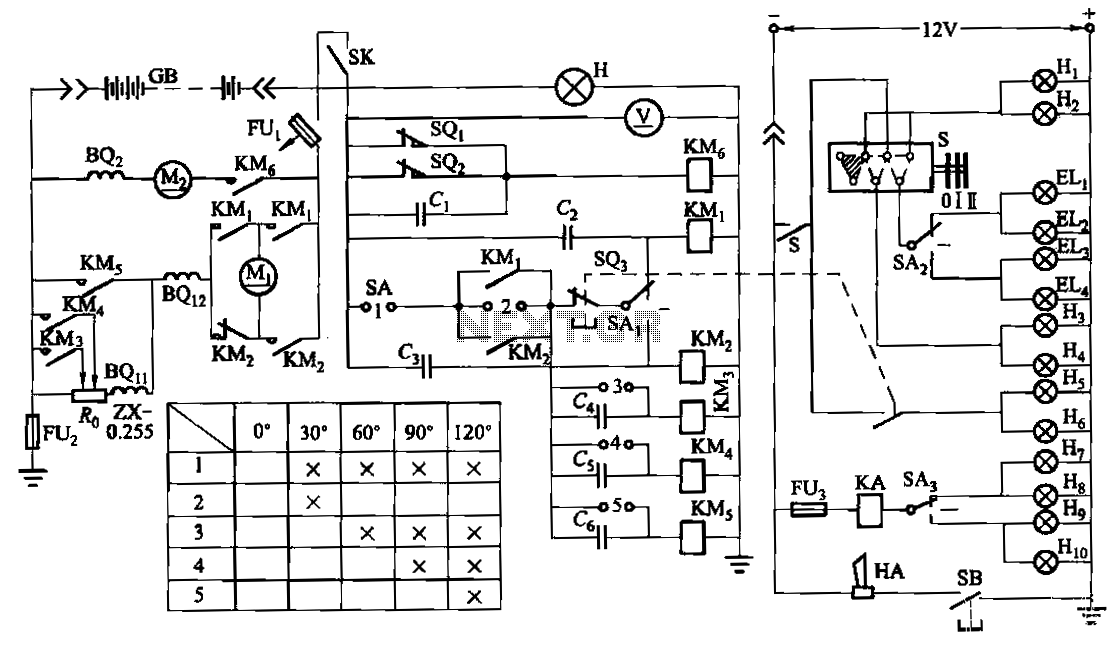
The forklift electric drive system comprises two DC series motors and associated control equipment. A 4.5 kW electric motor drives the vehicle through a mechanical transmission mechanism, enabling forward and backward movement of the forklift. A 6 kW pump...
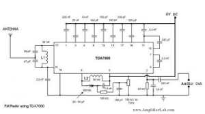
The following circuit illustrates a Single Chip FM Radio Circuit. This circuit is based on the IC TDA 7000 or TDA 7400. Features include a low-cost FM radio circuit. The Single Chip FM Radio Circuit utilizing the TDA 7000 or...
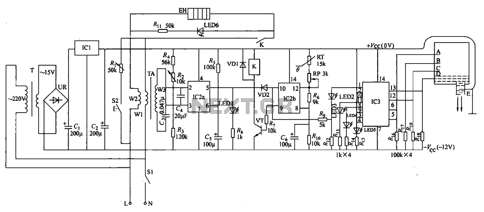
The electric water heater temperature control circuit includes functions for water level indication, temperature regulation, anti-dry protection, and automatic leakage power protection, ensuring safety and reliability. The circuit consists of a power circuit, leakage protection circuit, temperature control circuit,...
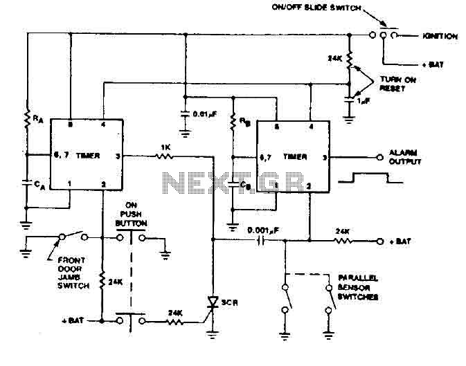
The 555 timer generates a reliable delay, enabling the driver to deactivate the alarm and eliminating the need for an external control switch that could be compromised. Additionally, the RCS prevents the activation of timer B unless it is...
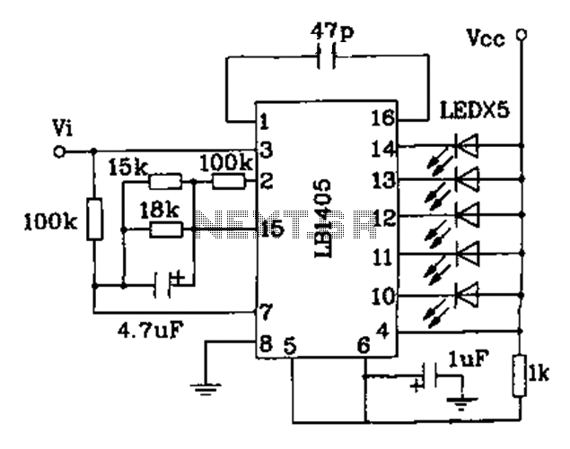
The LB140 is depicted in Figure as a typical driver IC circuit for a five-digit LED level indicator. The BL1405 is commonly utilized in tape recorders for level indication. The LB140 integrated circuit serves as a driver for five-digit LED...
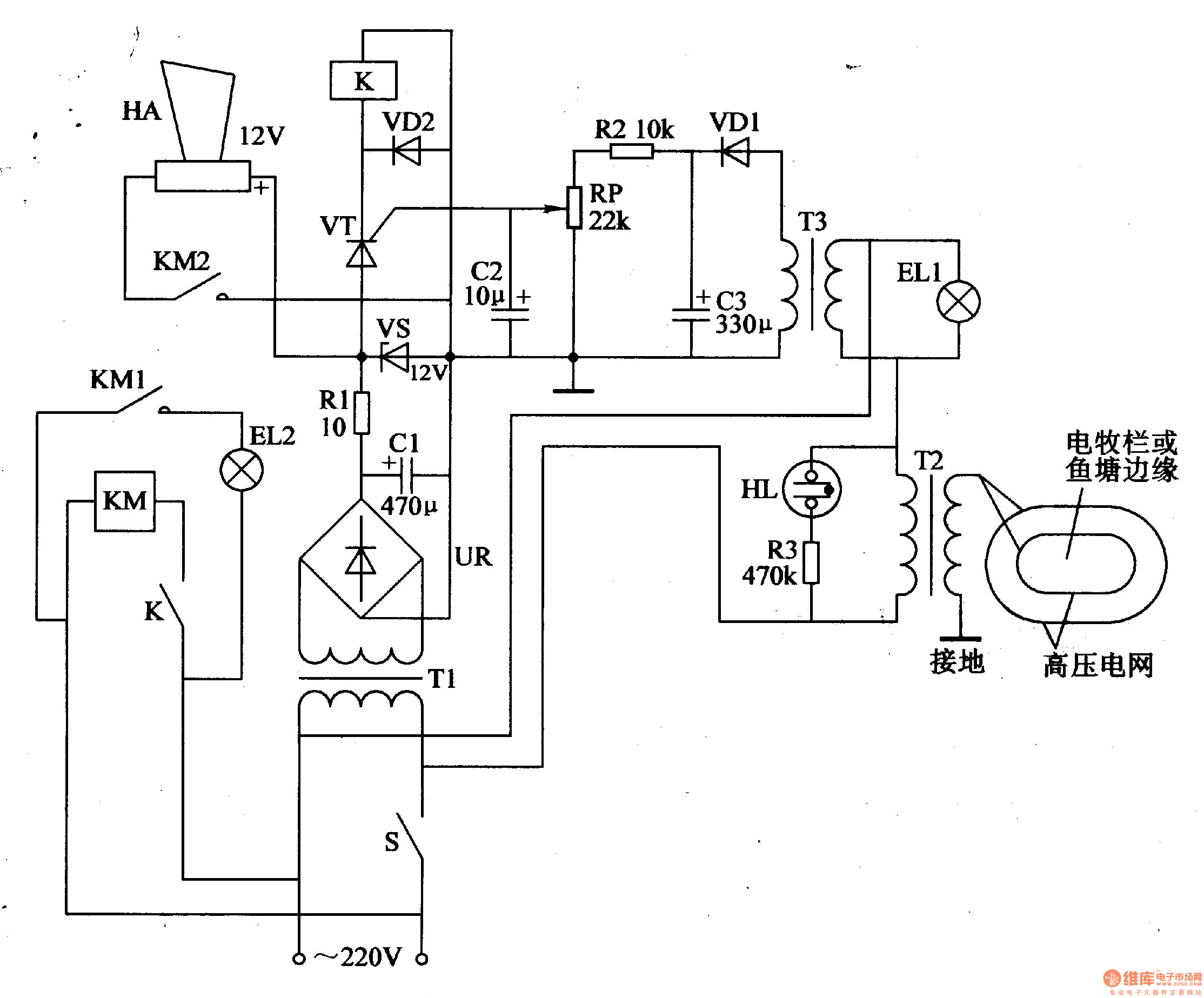
The electric fence control circuit consists of three main components: the power supply circuit, the high voltage circuit, and the sound and light alarm circuit, as illustrated in Figure 4-26. The power supply circuit includes a power switch (S),...