
Frequency doubler
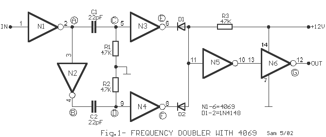
The described frequency doubler circuit utilizes a 4069 hex inverter IC, which is capable of performing multiple logic operations due to its six inverting gates. The input to the circuit is a square wave signal with a duty cycle close to 50%, which is essential for the proper functioning of the doubler. The voltage level of this input signal must be compatible with CMOS logic levels, typically ranging from 3V to 15V peak-to-peak, depending on the power supply used for the circuit.
The operation begins with the signal being fed into the first inverter (N1), where it is buffered and inverted. The output of N1 is a square wave signal that is 180 degrees out of phase with the input signal. This output is then fed into the second inverter (N2), which inverts the signal again, resulting in a second output that is also 180 degrees out of phase with the first output. The outputs from N1 and N2 are labeled as A and B, respectively.
To generate the necessary spike waveforms for frequency doubling, the outputs A and B are differentiated using capacitors (C1 and C2) and resistors (R1 and R2). This differentiation process generates two spike waveforms, labeled C and D, each 180 degrees out of phase with each other. These spike waveforms are then buffered, inverted, and shaped by the subsequent inverters (N3 and N4), preparing them for combination.
The critical step in frequency doubling occurs when the shaped signals from N3 and N4 are fed into a NOR gate configuration, which consists of diodes (D1 and D2), a resistor (R3), and the fifth inverter (N5). This NOR gate serves to combine the two spike waveforms effectively. The final output of the circuit is obtained by inverting the combined signal with the last inverter (N6), resulting in an output frequency that is twice that of the original input frequency.
The circuit is designed to operate over a broad frequency range, making it versatile for various applications. With the specified component values, the pulse width at the output points E and F is approximately 500 nanoseconds. This leads to a 50% duty cycle output when the input frequency is set at 500 kHz, thereby producing an output frequency of 1 MHz. This characteristic makes the frequency doubler circuit particularly useful in applications requiring frequency multiplication in digital and analog signal processing.This frequency doubler using a single 4069 hex inverter IC, a frequency doubler can be constructed to give an output pulse train whose frequency is twice that of a squarewave input signal. The signal is applied to the input of N1. It should be a squarewave with a duty-cycle of approximately 50% at level compatible with CMOS logic (3-15V peak to peak depending on supply voltage).
The input signal is buffered and inverted by N1, and inverted again by N2, so the outputs A and B of N1 and N2 are squarewave signals 180° out of phase. The output of N1, is differentiated by C1 and R1 and the output of N2 is differentiated by C2 and R2, giving two spike waveforms of C and D, 180° out of phase.
The signals are buffered, inverted and shaped by N3 and N4. These are then combined in a NOR gate consisting of D1, D2, R3 and N5, and finally inverted by N6 to give the frequency twice that of the input signal. The circuit will operate over a wide frequency range. With the component values shown the width of pulses in E and F point is about 500ns, so the duty cycle of the output will be 50% when the frequency is 1MHZ, when the input frequency is 500KHZ.By A.M.
Bosschaert 🔗 External reference
Related Circuits
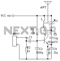
The ordinary triode 3DA87C is utilized to create a long-range FM transmitter circuit, which functions as a standard three-point oscillator circuit. This remote transmitter circuit is capable of large current emissions, achieving a range of up to 1 kilometer...
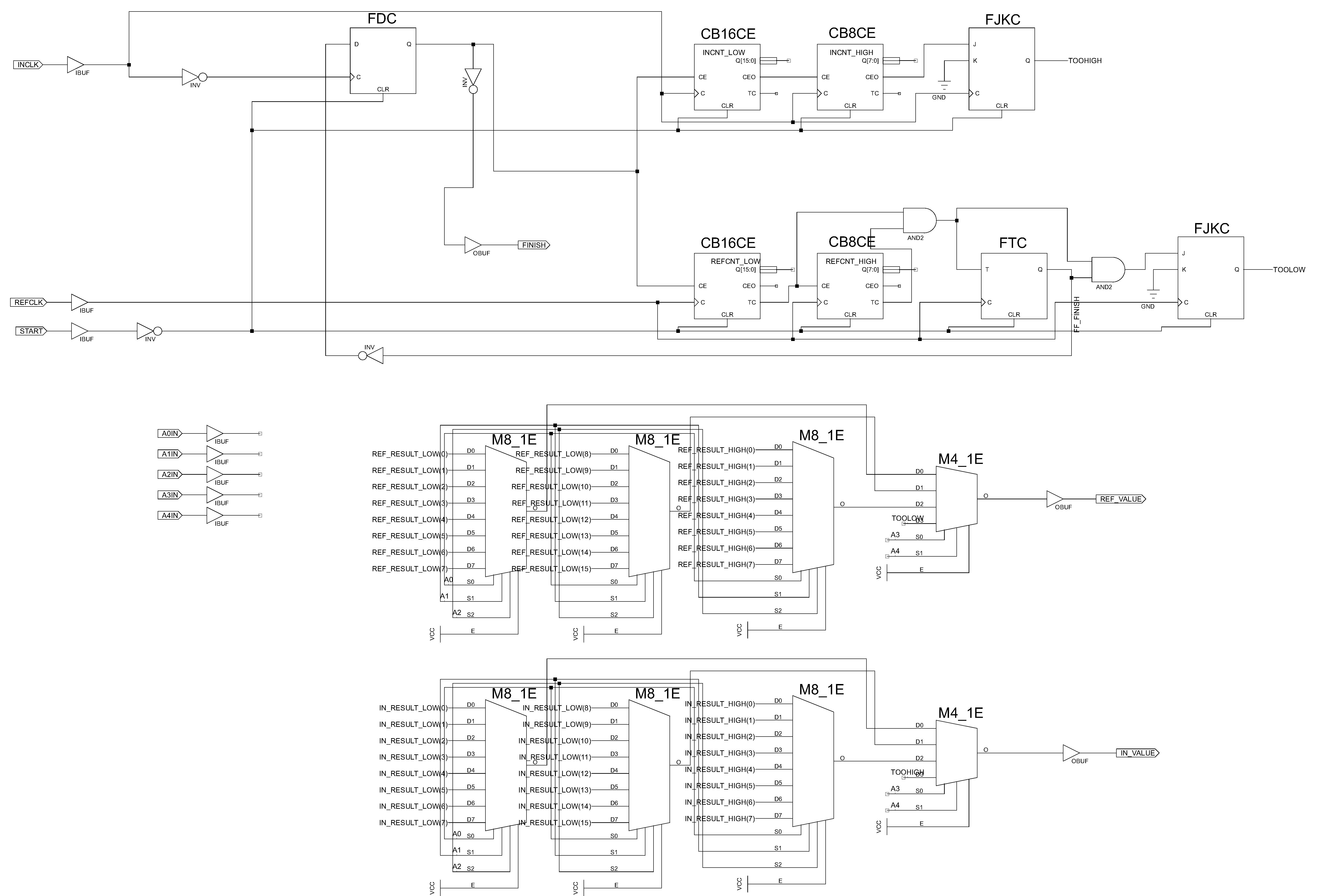
Connecting the CPLD board to a ChipKit board to enable the reading of the measured frequency. The connection between a Complex Programmable Logic Device (CPLD) board and a ChipKit board is essential for applications that require frequency measurement. The CPLD...
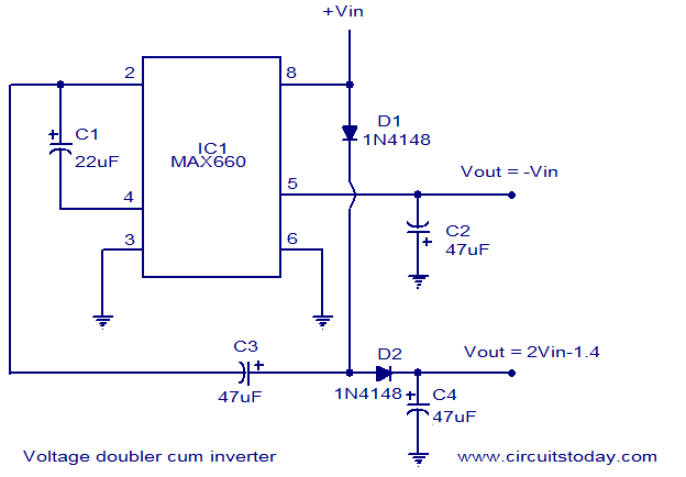
Voltage doubler circuit and voltage inverter circuit diagram with schematics using MAX660 IC, which is a DC voltage multiplier IC. This is a DC voltage doubler circuit and inverter. The MAX660 integrated circuit (IC) is designed for applications requiring a...
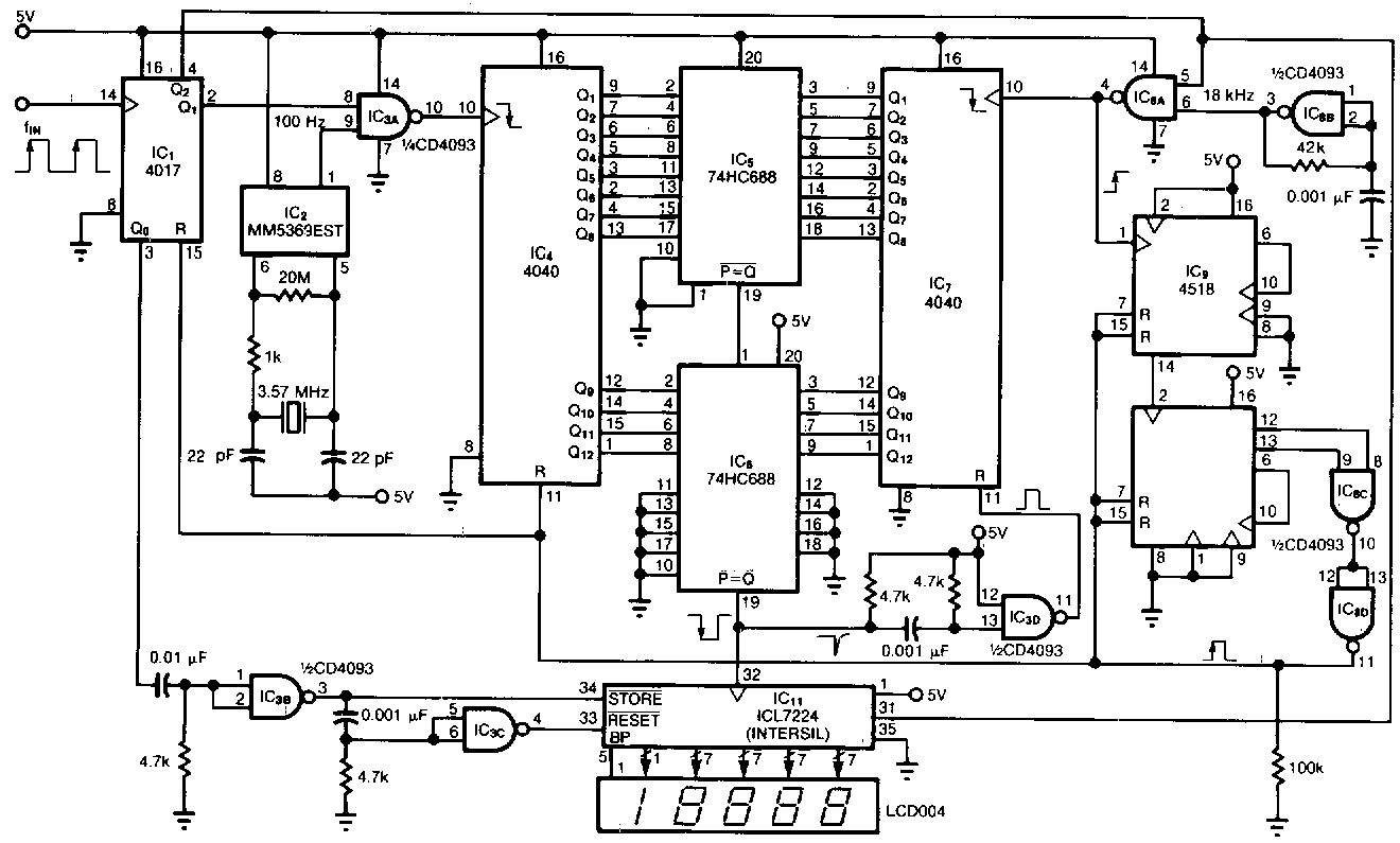
This tachometer measures heartbeats, respiratory rates, and other low-frequency events occurring at intervals ranging from 0.33 to 40.96 seconds. The circuit detects the period of the event, calculates the corresponding pulses per minute, and updates the LCD display accordingly....
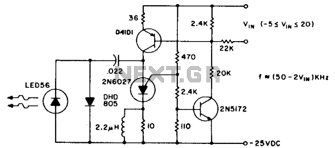
The pulse repetition rate is largely unaffected by temperature and power supply voltage, and it varies linearly with V1N, the modulating voltage. Effective information transfer was achieved at distances of 12 feet (~4m) in free air. A greater range...
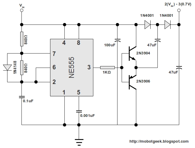
This DC voltage doubler circuit generates a voltage that is double its supply voltage. It is advantageous when a higher voltage level is required from a single lower voltage power supply. Due to the low current consumption in such...
Warning: include(partials/cookie-banner.php): Failed to open stream: Permission denied in /var/www/html/nextgr/view-circuit.php on line 713
Warning: include(): Failed opening 'partials/cookie-banner.php' for inclusion (include_path='.:/usr/share/php') in /var/www/html/nextgr/view-circuit.php on line 713