
Frequency to voltage converter
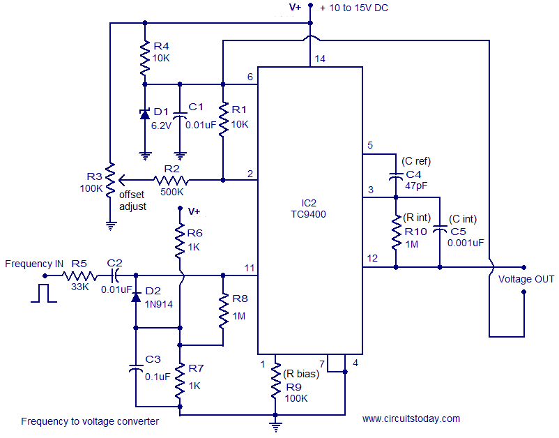
The TC9400 IC serves as a versatile component in this frequency-to-voltage conversion application, allowing for a compact and efficient design. The integration of various functional blocks within the IC minimizes the need for additional components, contributing to the overall simplicity and cost-effectiveness of the circuit. The output voltage's linear relationship with input frequency facilitates straightforward interfacing with other electronic systems, enabling the use of this converter in measurement and control applications. The calibration process ensures accurate performance, allowing users to adapt the circuit to specific input conditions and requirements. The careful selection of resistors and capacitors within the circuit is crucial for maintaining stability and precision in the output voltage, particularly in varying environmental conditions or with different input signal characteristics. The implementation of a clamp circuit enhances the robustness of the design, safeguarding the internal comparator from potentially damaging input signals. Overall, this frequency-to-voltage converter provides a reliable solution for applications requiring frequency measurement and conversion to voltage, with the TC9400 IC at its core offering both functionality and ease of use.A very simple and low cost frequency to voltage converter based on the TC9400 IC from Microchip is shown here. TC9400 can be either wired as a voltage to frequency converter or frequency to voltage converter and it requires minimum external components.
The functional blocks inside the TC9400 includes integrator opamp, 3uS delay circuit, one shot c ircuit, charge discharge control circuit, divide by 2 network and necessary drivers. This circuit finds application in a range of electronic projects like frequency meters, tachometers, speedometers, FM demodulators etc. In the circuit shown above the TC9400 is wired as a F to V converter that operates from a single supply.
The circuit generates an output voltage that is proportional to the input frequency. The input frequency is applied to the pin11 (non inverting input of the internal comparator). In order to trip the comparator the amplitude of the input frequency must be greater than +/-200mV. Below this level the circuit will not work at any situation. Whenever the input signal to the pin 11 of IC1 crosses zero to the negative direction the output of the internal comparator goes low. The 3uS delay circuit enables the Cref charge/discharge circuit after 3uS and this connects the Cref to the reference voltage and this charges the integrating capacitor Cint a specific amount of voltage.
In the single supply operation the reference voltage is the potential difference between pin 2 and 7 of the TC9400. Each time the input frequency wave form crosses zero towards positive direction, the output of the internal comparator goes high and this disables the Cref charge/discharge circuit which creates a short circuit across the Cref leads.
The voltage across the integrating capacitor Cint is retained because the only discharge path available is the 1M resistor Rint which is a too high and the voltage across Cint is the output voltage. Resistor Rbiasis used to set the bias current of the IC. The potential divider network comprising of R6 and R7 makes sure that the input threshold tracks the supply voltage always.
The clamp circuit using diode D2 prevents the input from going far negative in order to turn on the internal comparator. In simple words this section of the circuit can be generally termed as a level shifter. The TC9400 manufacturers claim that it can accept a signal of any frequency at its input. In the practical side, for the proper working of this circuit the positive half of the input signal must have at least 5uS pulse width and for the negative half it must be greater than or equal to 5uS.
For calibration adjust the offset adjust trimpot to obtain 0V at the output with no input frequency applied. If you have a function generator, set frequency input to 10KHz and make adjustments in the value of Cref to get around 2.
5 to 3 volts at the output. This calibration is meant for a maximum input frequency of 10KHz. In the circuit the inverting input of the internal comparator is referenced to 6. 2V by using D1. So the input signals amplitude must be between 4V and the supply voltage (V+). The output voltage and input frequency of the F to V converter is related using the equation V out = V ref x C ref x F in where V out is the output voltage and F in is the input frequency. 🔗 External reference
Related Circuits
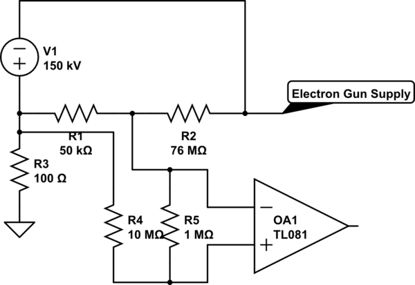
A high voltage power supply is designed for an electron beam system. The voltage regulator utilizes an outdated analog system that operates through a comparator and a reference signal from a potentiometer (POT). The challenge involves the feedback voltage...
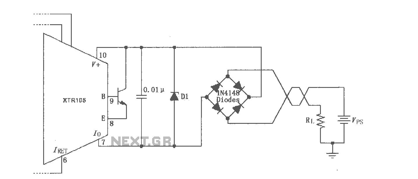
The XTR105 reverse voltage and over-voltage surge protection circuit is illustrated. A Zener diode rated at 36V can be utilized, with options including 1N4753A or 1N6286A. The maximum supply voltage (Vps) should be less than the minimum breakdown voltage...
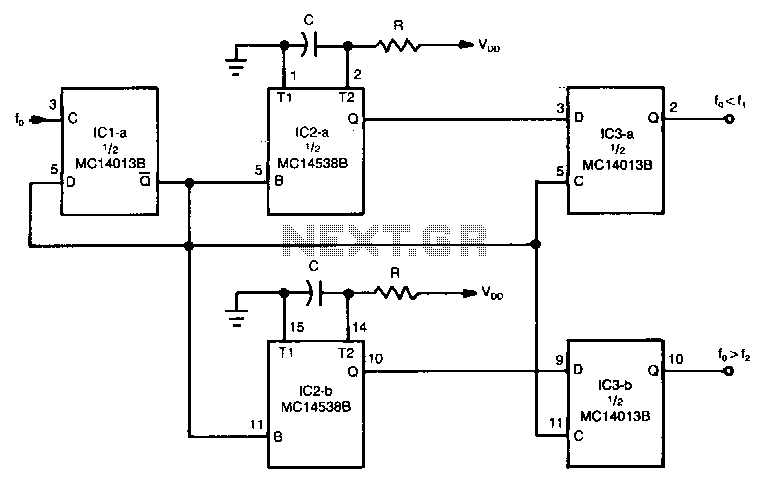
The circuit can be used to determine whether an input signal falls within a specific frequency range. The device comprises three integrated circuits (ICs), including a dual monostable multivibrator and two dual D-type flip-flops. The signal whose frequency is...
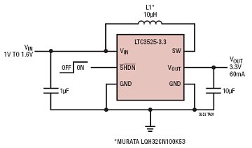
The LTC3525-3/LTC3525-3.3/LTC3525-5 are high-efficiency synchronous step-up DC/DC converters with output disconnect capability that can operate with an input voltage as low as 1V. These converters provide a compact and efficient alternative to charge pumps for single-cell or dual-cell alkaline...
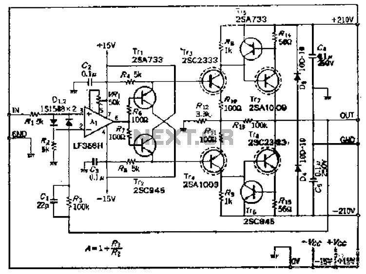
This amplifier circuit operates with an OP amplifier that is power-driven, which leads to the presence of floating voltage errors and necessitates a high-pressure booster for transistor protection. The circuit utilizes a mutual feedback configuration, connecting to the output...
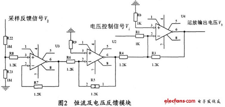
The output current range of the parameter current regulator is limited, and its precision is not high. Connecting the feedback adjustment type output current of the current-stabilized power source in series results in lower efficiency. The steady current source...
Warning: include(partials/cookie-banner.php): Failed to open stream: Permission denied in /var/www/html/nextgr/view-circuit.php on line 713
Warning: include(): Failed opening 'partials/cookie-banner.php' for inclusion (include_path='.:/usr/share/php') in /var/www/html/nextgr/view-circuit.php on line 713