
Function Generator 1

The function generator circuit primarily comprises a triangle wave generator, which is essential for producing the desired waveforms. The triangle wave is generated through a capacitor that is charged and discharged at a constant current, ensuring a linear ramp. The integration of the current by the capacitor results in a ramp voltage that oscillates between defined thresholds, which are monitored by comparators. These comparators trigger the SR flip-flop that controls the output waveform. The use of an op-amp integrator in the circuit allows for precise control over the ramp characteristics. The voltage-controlled switch enables smooth transitions between positive and negative ramps based on the flip-flop's output state. This configuration facilitates the generation of various waveforms, making the function generator a versatile tool in electronic testing and experimentation. By manipulating component values, such as resistors and capacitance, the frequency and amplitude of the generated waveforms can be adjusted to meet specific testing requirements. The ability to visualize output signals through simulation aids in understanding the circuit's behavior and performance, providing valuable insights into the operation of the function generator.At some time, you`ve probably run into this magical instrument in the lab - the function generator. Just turn the waveform selector knob and a triangle, square or sine wave appears at the output! Turn another knob and the frequency of the signal changes. Now you can feed the square wave into an amplifier you`re testing to see how quickly it respon ds. Is there any over shoot or ringing Or maybe you`re testing an audio amplifier and you feed it a 1 kHz sine wave. Is there any distortion at the output I looked at my handy function generator and wondered what kind of circuit creates these waveforms A search on the web produced a few schematics.
Although they all took different circuit approaches, the essence of each one resembled the overall topology shown above. At the core of the function generator is a triangle wave generator. How do you generate a triangle wave The most common way is to get a capacitor and then alternate charging it and discharging it.
But how to you get a nice linear ramp across the capacitor The key here is to charge and discharge it with a constant current source. Mathematically, here`s how it works. A capacitor integrates a current, i. Looking at function generator schematics you`ll find different ways to implement constant current sources and integrators.
One circuit uses the classic op amp integrator. To create the negative ramp, the circuit looks like this. In the SPICE circuit, vs and R1=10k set up I1. An inverter XOP2 creates -vs from vs. I2 is created using voltage -vs and with R2=5k. R2 is switched into the circuit by voltage-controlled switch S1. The integrator is created by XOP1 and CI. The next challenge is switching between the positive and negative ramps. Typically, two voltage thresholds (high and low) are created to set the boundaries of the ramp voltages. RTH1 and RTH2 set the positive threshold Vth_HI=+2. 5V, while RTH3 and RTH3 set the negative threshold Comparator XCMP1 compares the ramp voltage to Vth_HI.
XCMP1`s output goes from LO to HI when vo reaches Vth_HI=+2. 5V. Likewise, XCMP2`s output goes from LO to HI to high when vo reaches to Vth_LO=-2. 5V. The outputs of XCMP1 and XCMP2 are fed to the Set and Reset input of the flip-flop. Positive edges at the Set and Reset inputs will set the flip-flop output HI or LO, respectively. Why use the SR flip-flop The Flip-Flop`s output serves as the square wave output. It also controls the S1. The state of of S1 (ON or OFF) determines if op amp XOP1 is generating a positive or negative ramp. Although the RS Flip-Flop can be modeled in many ways, the classic cross-coupled NAND gate defines this function. Furthermore, the NANDs were created from simple switches so running the SPICE file does not require a mixed-mode (analog / digital) simulator.
Let`s design a function generator and take it out for a spin. Suppose you are asked to generate a 1 kHz triangle wave (To=1. 0 ms). Initially set VS=1V, R=10k, R2=5k, Vth_HI=+2. 5V, Vth_LO=-2. 5V. The thresholds imply that the negative ramp will change by Now the big question is this: what C do we need such that vo will change -5V in †t = To/2 = 0. 5 ms Starting with †vo = vs / R · †t / C we solve for C. CIRCUIT INSIGHT Run a transient simulation and plot the output V(3). Does the output ramp linearly up and down between the thresholds +2. 5V and -2. 5V Way cool! I still get a kick out of seeing signal generators do their thing. In the same window, plot the comparator`s outputs V(11) and V(12). You can see the outputs flip state as the ramp exceeds the upper or lower threshold. However, the ramp quickly direction and the comparator output changes state, leaving only a narrow pulse.
The flip-flop`s output V(15) controls the state of the switch S1. When V(15) goes LO, S1 turns ON creating a POS ramp. When V(15) goes HI, S1 turns OFF creating a NEG ramp. Try changing CI by 10x or 0. 1x of its value. Will this create a faster or slower ramp This i 🔗 External reference
Related Circuits

The circuit utilizes two unijunction transistors. The low-frequency sawtooth generated by Q1 modulates the high-frequency tone produced by Q2. The output is designed to feed into a high-impedance amplifier. Both Q1 and Q2 are 2N4871 transistors. The circuit comprises two...
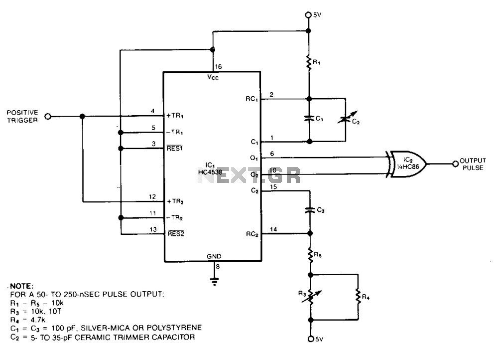
The pulse generator consists of two low-power CMOS chips that produce a precise pulse width ranging from 50 to 500 ns. IC1 is a dual monostable multivibrator (one shot) where each positive trigger pulse initiates simultaneous positive output pulses...
This is a simple home telephone ringtone generator circuit constructed using only a few electronic components. It generates a simulated telephone ringtone and requires a DC supply voltage ranging from 4.5V to 12V. This circuit can be used in...
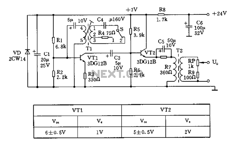
The 450/800Hz oscillation circuit depicted in the figure utilizes transformer coupling. The frequency conversion is achieved by varying the inductance through a variable filter tap (T1). When the switch control signal (S) is set to position 1, the oscillator...
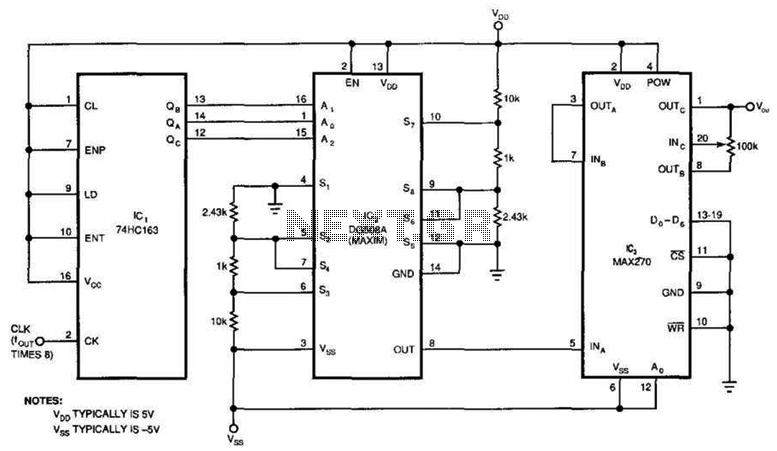
This circuit generates a pure sine wave with a total harmonic distortion (THD) of -80 dB and a frequency equal to the cutoff frequency (fc) of the filter in IC3. It utilizes a counter, an 8-channel analog multiplexer, and...
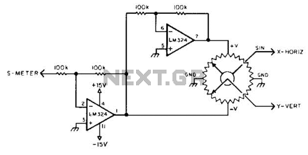
To display polar quantities, which include both the magnitude and direction of a received radio signal, a sine and cosine voltage proportional to an angle corresponding to the antenna direction is required. This setup utilizes a sine-cosine potentiometer connected...