
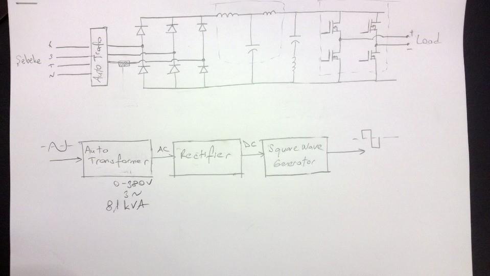
High Power Square Wave Generator (0-500V 25A)
In this circuit design, two voltage sources, V1 and V2, are essential for the operation of the system. The selection of either 5V or 10V for these sources is crucial, as it impacts the overall efficiency and complexity of the circuit. Utilizing a higher voltage may reduce the number of required power supplies, simplifying the design. The use of logic level FETs is recommended if they are available at the required voltage, as they can provide efficient switching capabilities.
For applications with a low switching frequency (up to 100 Hz), Silicon Controlled Rectifiers (SCRs) or similar devices are advantageous due to their ability to handle high power and provide robust performance in inverter applications. SCRs can effectively generate stepped square waves, which serve to approximate a sine wave output, making them suitable for power applications where waveform quality is less critical.
The incorporation of solid-state relays in parallel can enhance the circuit's ability to manage high currents. This configuration is beneficial as it minimizes the voltage drop across the relays when they are in the ON state, ensuring that the load receives the maximum possible voltage. Furthermore, when the relays are OFF, they present a very high impedance, resulting in negligible current flow, which is advantageous for power savings and reducing heat generation.
The most significant challenge in this design is generating a 500V DC rail capable of delivering 25A of current. This requirement translates to a minimum average power output of 6250W. Considering a 50% duty cycle, the effective power requirement may exceed 7kW when factoring in losses within the system. Therefore, careful attention must be given to the design of the power supply and the components used to ensure they can handle the expected load without failure. Proper thermal management and component ratings must be considered to maintain reliability and efficiency in the overall circuit operation.V1 and V2 are set to 5V in the simulation, but could also be 10V to eliminate the need for a second supply ” or, if you can find logic level FETs at that high a voltage, then you can reduce the 10 volt supply to 5 volts. Assuming that the switching frequency is low enough (100 Hz max), why not use SCRs or a similar class of devices I believe these would be better
suited to this kind of work (they are used in inverters to generate stepped square waves to approximate a sine wave). Also perhaps a paralleled combination of solid-state relays might be able to handle the total current this will probably be better than the H-bridge MOSFET scheme since the relays will appear in series with the load and won`t have much drop across them when ON.
When OFF, the current will be almost nil. The main problem is to first generate the 500V DC rail at 25A that represents minimum or average power requirement of 6250W assuming 50% duty cycle almost 7kW+ when we consider losses. 🔗 External reference
Related Circuits
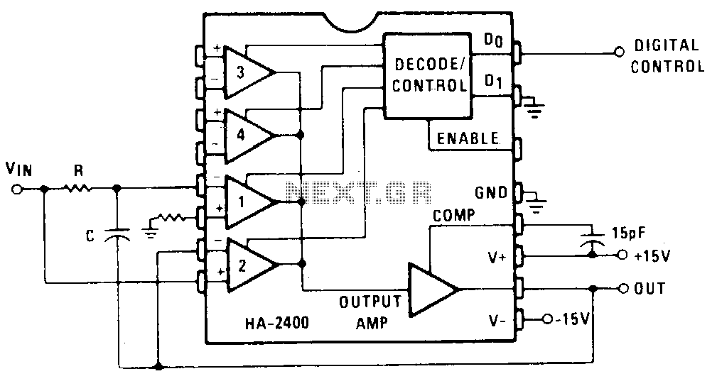
Channel 1 is configured as a conventional integrator, while Channel 2 is set up as a voltage follower. When Channel 2 is activated, the output will track the voltage of VJN, and capacitor C will discharge to maintain 0...
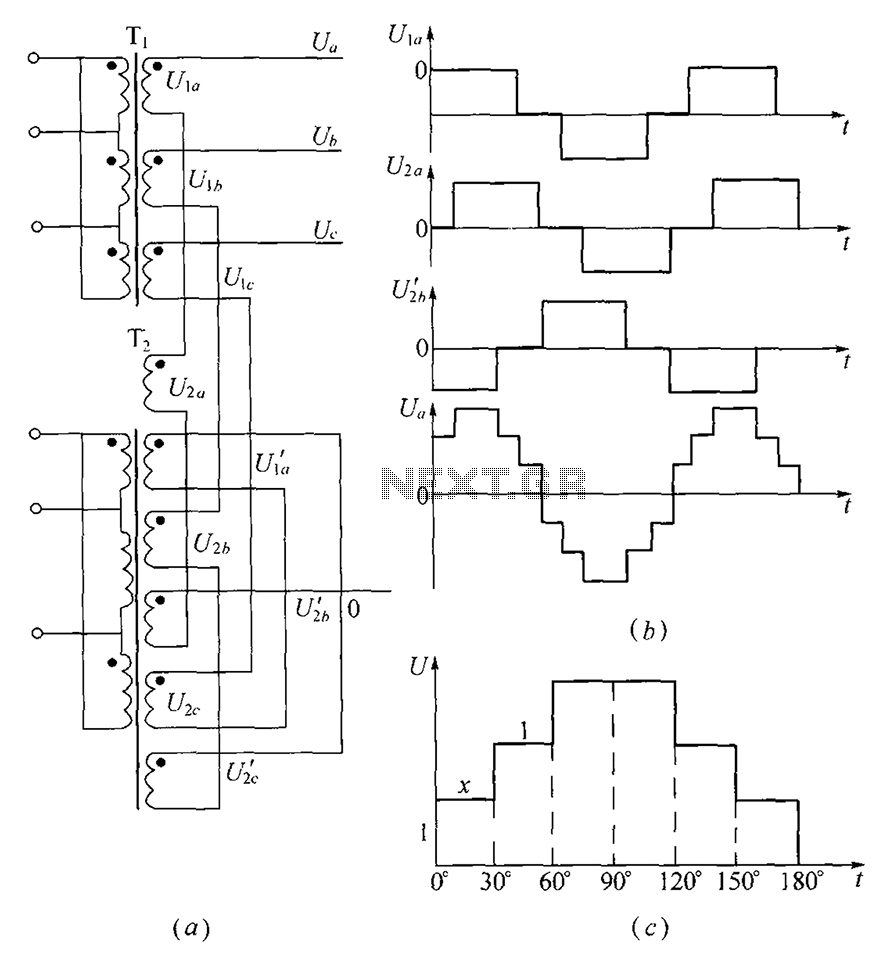
As shown, (a) for the three-phase step wave inverter output transformer winding connections; (b) in the figure, its output waveform. The three-phase step wave inverter is designed to convert direct current (DC) into a three-phase alternating current (AC) output. This...
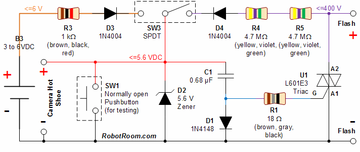
This circuit incorporates a datasheet-compliant trigger signal, reversed polarity protection, an optional test button, and the capability for battery operation. It utilizes either the U1 L601E3 or MAC97A8 triac, rated for 400 V and 1 A. When U1 is...
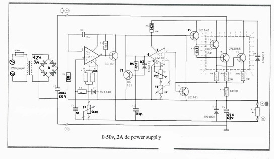
A variable power supply designed for laboratory use. It utilizes two integrated circuits (ICs) to provide adjustable output voltage and current. This variable power supply is engineered to meet the diverse needs of laboratory applications, offering flexibility in output voltage...
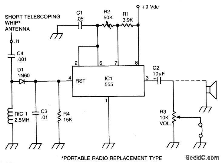
A sidetone oscillator is a specialized audio oscillator that is activated and deactivated in conjunction with the transmitter. This oscillator is driven by RF signals and is powered by batteries. It employs a 555 integrated circuit (IC) timer configured...
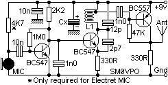
My FM Wireless Microphone has been a very popular project with beginners and experienced constructors alike. It has been used inside guitars and as the basis of a remote control system. I do however, receive many requests for a...