
High Precision Voltage-to-Frequency Converter (VFC) Using CA3130 Op-Amps
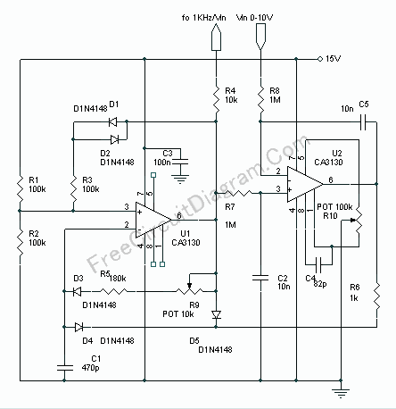
The circuit operates by converting an input voltage into a frequency signal, which is particularly useful for applications requiring the transmission of analog signals over radio frequency channels. The use of CA3130 op-amps ensures low offset voltage and high input impedance, which is essential for accurate voltage sensing, especially in temperature measurement scenarios.
The charging and discharging of capacitor C1 create a timing mechanism that directly relates to the input voltage level. The hysteresis introduced by resistor R3 prevents rapid oscillations of the output and ensures stable operation. The feedback loop involving U2 allows for dynamic control of the discharging rate of C1, enabling the pulse frequency to vary according to the input voltage.
The diodes D3 and D4 play a critical role in isolating the charging and discharging paths, ensuring that the circuit maintains accuracy despite temperature variations. The additional components, D1, D2, and R3, are necessary for compensating the effects of temperature on the diode characteristics, thereby stabilizing the circuit’s performance over varying environmental conditions.
Overall, this voltage-to-frequency converter circuit is a robust solution for applications in telemetry and remote sensing, where reliable transmission of analog signals is required. By fine-tuning the circuit parameters, such as the values of R9 and R10, the design can be adapted to meet specific operational requirements, ensuring optimal performance in real-world applications.Voltage to frequency is very useful in many situation, such as transmitting temperature measurement using standard voice radio transceiver. This circuit (see the circuit`s schematic diagram) uses only two CA3130 op-amps, but the performance is good enough.
The linearity of the voltage-frequency transfer is better than 0. 5% and the temperature coef ficient is lower than 0. 01% ! Assume that the output voltage of U1 is 15V, C1 will be charged with time constant (R9 R5)C1, flowing through R9, R5, D3, and C1. This charging will continue until the voltage of pin 2 (U1) get higher than the non-inverting input voltage at pin 3.
After this, the output voltage of U1 will drop to zero (ground) and the non-inverting input pin 3 will drop to about 5V, set by the R3 for hysteresis. Now C1 will discharge its current through D4 and R6, at a rate determined by the voltage level at U2 output.
If the C1 voltage has decreased below 5 volt then the U1 output will swing to 15V and the cycle will be restarted. At U1 positive input, the voltage level is the average of the pulse output of U1. The output of U1 is a positive pulse with constant width, and the space is variable depends on the discharging rate of C1 which is depend on U2 output.
If the voltage level of this positive input of U2 is smaller than the control voltage at the negative input then the output of U2 will decreased toward negative supply (ground), therefore the discharging rate of C1 will be increased and the pulse output of the U1 will have shorter space, thus increase the voltage level at C3 until the it`s equal to the control voltage level at negative input of U2. If the voltage level at positive input is higher than the negative input, then the output of U2 will increase toward positive supply (15V) giving a reversed action to keep the level of negative and the positive input equal.
Because D3 and D4 are needed to separate the charging and discharging control of C1, and the diodes have different characteristics at different temperature, D1, D2, and R3 are provided to introduce similar reference voltage variation of positive input as seen in the negative voltage variation caused by D3 and D4 at different temperatures. Use R10 pot to correct the offset error of U2 and R9 to fine tune the voltage-to-frequency conversion rate to exactly 1kHz/Volt.
[Schematic Source: RCA Application Note] 🔗 External reference
Related Circuits
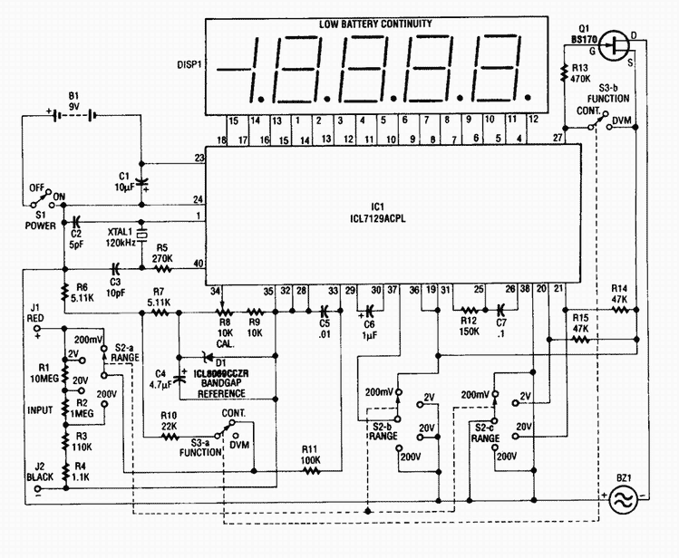
This 4 1/2-digit DVM circuit is built around a Maxim ICL7129ACPL A/D converter and LCD driver. An ICL8069 CCZR 1.2-V band-gap reference diode is used for a voltage reference. S2a-b-c select one of four ranges up to 200 V...
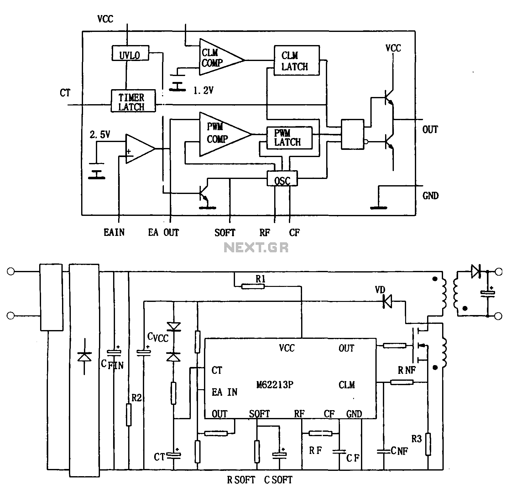
Figure (a) illustrates a block diagram of the internal architecture of the M62213FP, which is a high-speed switching power supply controller. This device includes an oscillator, PWM comparator, error amplifier, output circuit, over-voltage protection, timing latch circuit, over-current protection...
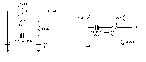
Below are a couple circuits you can use to produce a 32.768 KHz square wave from a common watch crystal. The output can be fed to a 15 stage binary counter to obtain a 1 second square wave. The...
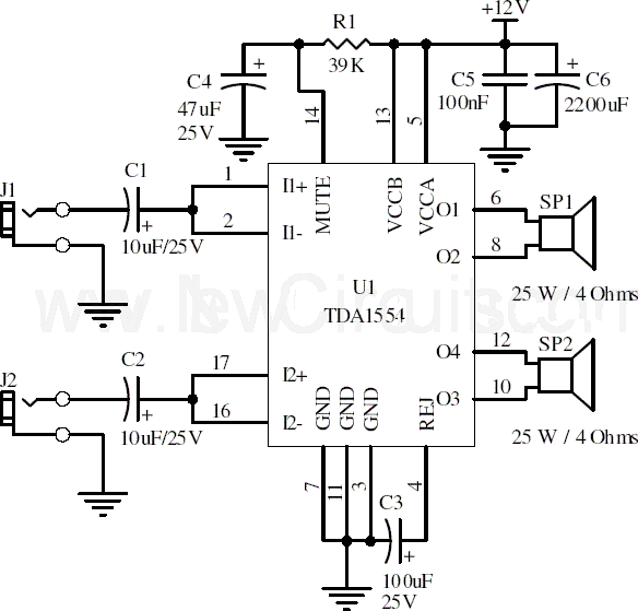
This document presents a 22-watt stereo audio power amplifier circuit diagram utilizing the TDA1554 integrated circuit from NXP Semiconductors (formerly known as PHILIPS Semiconductors). The circuit is designed to amplify stereo signals effectively. It dissipates approximately 28 watts of...
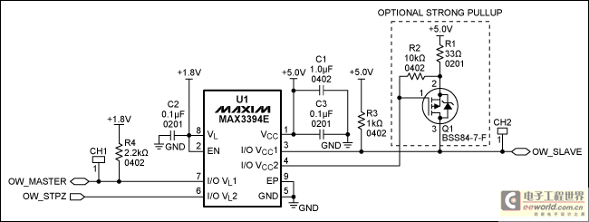
The designer requires a 1-Wire host computer IO framework that operates at 1.8V. Most 1-Wire devices are unable to function at this voltage. This application recommends implementing a 1.8V 1-Wire host computer alongside a 5V 1-Wire reference design for...
Automated instrumentation wiring using interference filters for the inverter is not as effective for harmonic processing. When operational, it will radiate a strong field strength due to high amplitude electromagnetic waves. If the meter is installed in the automation...
Warning: include(partials/cookie-banner.php): Failed to open stream: Permission denied in /var/www/html/nextgr/view-circuit.php on line 713
Warning: include(): Failed opening 'partials/cookie-banner.php' for inclusion (include_path='.:/usr/share/php') in /var/www/html/nextgr/view-circuit.php on line 713