
IC Adder Chip
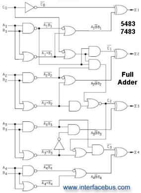
The 4-bit adder circuit is a fundamental digital component used in arithmetic operations, particularly in binary addition. It consists of four full adders connected in series, where the output carry from each full adder serves as the carry input for the next significant bit. Each full adder takes three inputs: two binary digits (A and B) and a carry-in (Cin). The outputs are the sum (S) and the carry-out (Cout).
The full adder can be implemented using basic logic gates: XOR, AND, and OR gates. The sum output can be expressed as S = A XOR B XOR Cin, while the carry-out is given by Cout = (A AND B) OR (Cin AND (A XOR B)). This allows the circuit to handle the addition of binary numbers correctly, including cases where the addition results in a carry.
In the context of integrated circuits, the 54LS83 and 54283 are popular choices for implementing 4-bit adders. The 54LS83 is designed for commercial applications, while the 54283 is intended for military use, featuring a wider operational temperature range. Both ICs share similar functionalities and pin configurations, ensuring compatibility in circuit designs, albeit with attention to the specific package styles and temperature ratings.
When designing a circuit that includes a 4-bit adder, it is crucial to consider the supply voltage, input signal levels, and the desired operational temperature range. The choice between the 54LS83 and 54283 should be made based on the application's environmental requirements. Proper layout practices, including minimizing trace lengths and ensuring adequate power supply decoupling, will enhance the performance and reliability of the 4-bit adder circuit.A 4-bit adder which adds two four bit binary numbers with a Carry in line. The diagram above show the logic gate schematic of a 4-bit adder. A full adder take in two number and a carry in line, while a half adder does not allow a carry-in bit. Although both a full adder and a full adder will output a carry out bit. Note the Carry Out is not shown in the diagram above. This schematic link shows the transistor view of a 4-bit adder circuit. A 5483 diagram is shown as an example, but there is no difference between the functions of a 5483 and a 54283 part. Both [xx83 and xx283] components are electrically and functionally identical, however they do differ in their pin out.
So a 54LS83 will not function in a circuit layed out for a 54LS283 part. There is also no difference between a Commercial Temperature range; 74283 and a Military Temperature range; 54283. The pin out is the same and they are also electrically and functionally identical. They also have the same pin out or pin lay-out when both are selected using the same package. However the package styles offered for the 74283 and the 54283 functions may be different. The only real difference between the two ICs is that the 54xx version will operate to a higher temperature than the 74xx version.
🔗 External reference
Related Circuits
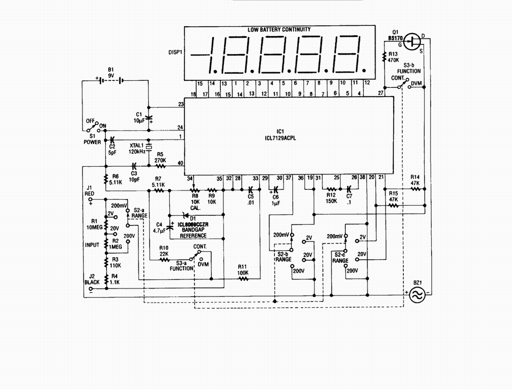
Single-chip digital voltmeter. This 4 1/2-digit DVM circuit is built around a Maxim ICL7129ACPL A/D converter and LCD driver. An ICL8069 CCZR 1.2-V band-gap reference diode is used for accuracy. The described circuit is a single-chip digital voltmeter (DVM) utilizing...
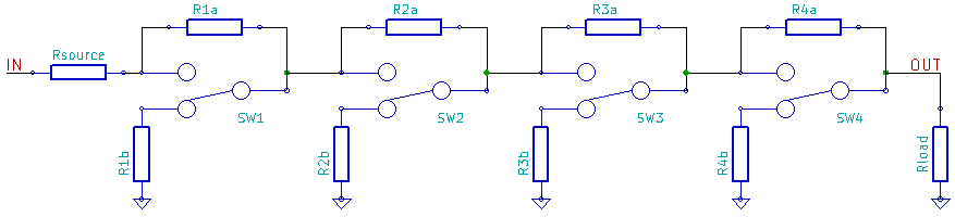
A logarithmic resistor ladder is an electronic circuit consisting of a series of resistors and switches, designed to create attenuation from an input to an output signal, where the logarithm of the attenuation ratio corresponds to a digital code...
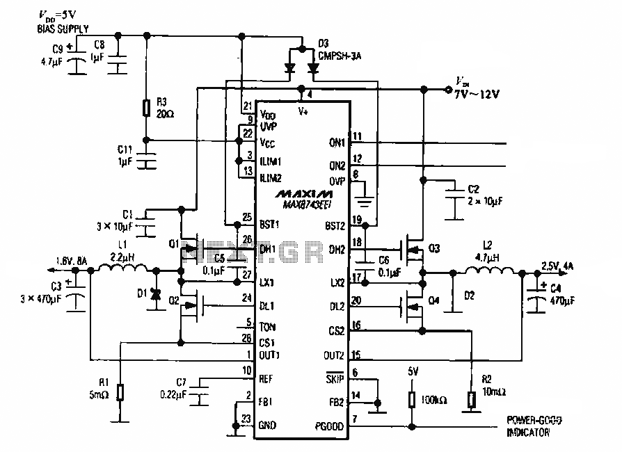
The circuit utilizes the MAX8743 chip for a laptop chipset power supply. It demonstrates the conversion of a 5V power supply into +2.5V and +1.8V outputs. The MAX8743 is a highly integrated power management solution designed specifically for laptop chipsets....
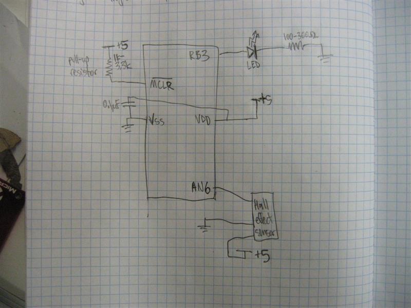
Refer to the OSCCON register in the datasheet (currently on page 19). This register controls the speed of the internal clock, which operates at 31 kHz upon startup—considered too slow. By using the OSCCON register, the speed can be...
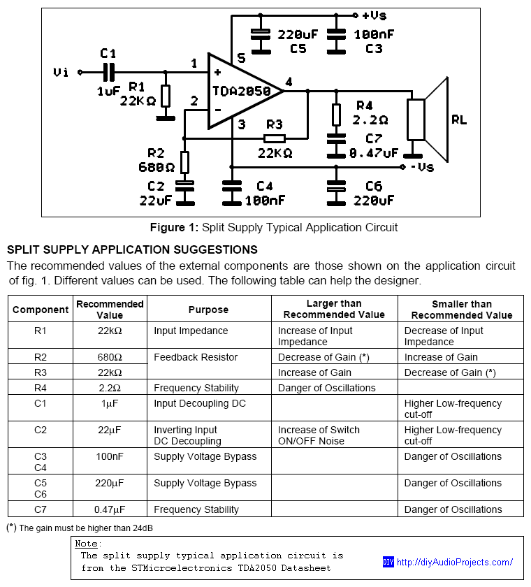
DIY TDA2050 Non-Inverting Chip Amplifier project constructed on a protoboard. The TDA2050 is a popular audio power amplifier integrated circuit designed for various audio applications. This non-inverting amplifier configuration is particularly valued for its simplicity and effectiveness in delivering high-quality...
The AC input circuit functions as a converter, transforming an alternating current (AC) signal into a direct current (DC) signal, which is subsequently processed by an analog-to-digital (A/D) converter chip. The input circuit is designed to handle AC signals, typically...