
KA2213 single chip sound recorder or reproducer integrated circuit diagram
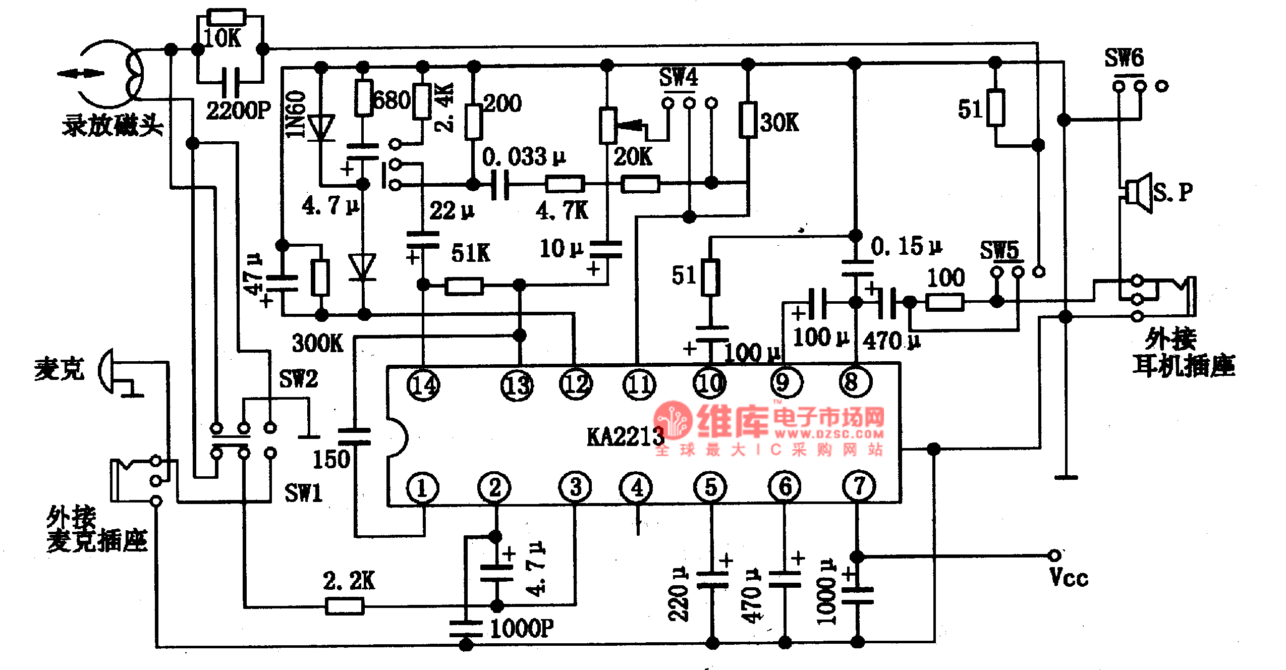
The KA2213 integrated circuit is designed for efficient audio recording and playback applications, making it suitable for various audio devices such as cassette recorders, mini-disc players, and other audio equipment. The internal architecture is optimized for high fidelity, featuring a record and playback preamplifier that boosts audio signals to appropriate levels for processing. The automatic gain control (ALC) circuitry ensures consistent output levels by adjusting the gain based on the input signal strength, which is essential for maintaining audio clarity during playback and recording.
The power amplifier circuit within the KA2213 is engineered to drive speakers or headphones directly, providing sufficient power output while minimizing distortion. The ripple filter circuit serves to reduce noise and interference, enhancing the overall audio quality. The 14-pin dual in-line package design facilitates easy integration into existing electronic systems, while the cooling ribs help dissipate heat generated during operation, ensuring reliable performance.
In practical applications, the KA2213 can be connected to various input sources, such as microphones or line-level audio signals, and can interface seamlessly with other components in a sound system. The switches SW1 to SW6 allow users to easily toggle between recording and playback modes, providing intuitive control over the device's functionality. The absence of a flux imbalance circuit in the typical application diagram indicates a simplified design, focusing on essential features for standard audio applications. This design approach makes the KA2213 a versatile choice for engineers and designers seeking reliable audio performance in their projects.KA2213 is a single chip record and play back integrated circuit which is produced by South Korea`s Samung, it is used in recorder and unit audio. 1, KA2213 internal circuit block diagram and pin function KA2213 internal block contains a record and play back preamplifier, a power amplifier circuit, a automatically gain control circuit(ALC)and ripple filter circuit.
The internal block internal circuit block diagram is shown in the figure 1-1. Reading IC adopts 14-foot dual in-line package, it has cooling ribs. The integrated circuit pin function and data is shown in the chart 1-1. Figure 1-1, the internal block internal circuit block diagram is shown. 2, KA2213 typical application circuit KA2213 internal block typical application circuit is shown in the figure 1-2. The figure has no flux imbalance circuit. SW1-SW6 is record and play back switch, the graphic position is in sound-reproducing state. Figure 2-2, KA2213 internal block typical application circuit 🔗 External reference
Related Circuits
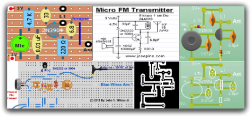
Radio-Circuits has elevated the standard with this website. Unlike any other circuit site on the internet, they have compiled ten of the most popular FM transmitter circuits. Radio-Circuits provides a comprehensive collection of FM transmitter circuits, showcasing a variety of...
This circuit diagram of a UPS is designed for use with cordless telephones that cannot operate during a power failure. Since the UPS is intended solely for telephones, its output power is limited to 1.5W. This UPS circuit is...
The circuit utilizes a 555 IC in conjunction with capacitors C1, C2, and a metal plate (tablet) M to create a distributed capacitance Co and resistor R1 connected to ground. Resistor R2 forms a self-excited multivibrator, while resistors R3...
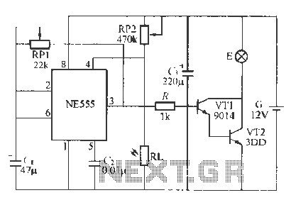
This circuit utilizes battery-powered blinking warning lights for roadblocks. It can operate on AC power to create barricades with warning indicators. The circuit incorporates an NE555 timer and resistors RP1 and RP2, along with resistor R1, to form a...
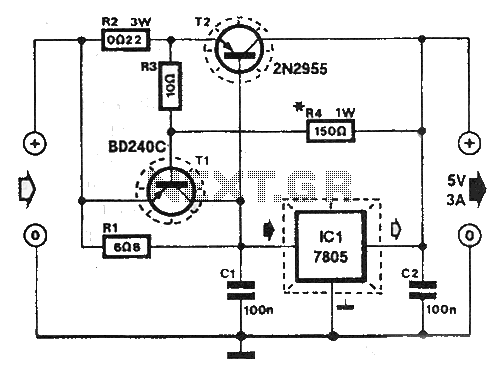
At this voltage regulator prototype the maximum current, with output shortcircuited it was only 0.5 A, so no overheating occurred. In this DC voltage regulator circuit, T1 is for current limitation. As soon as the voltage on the R2...
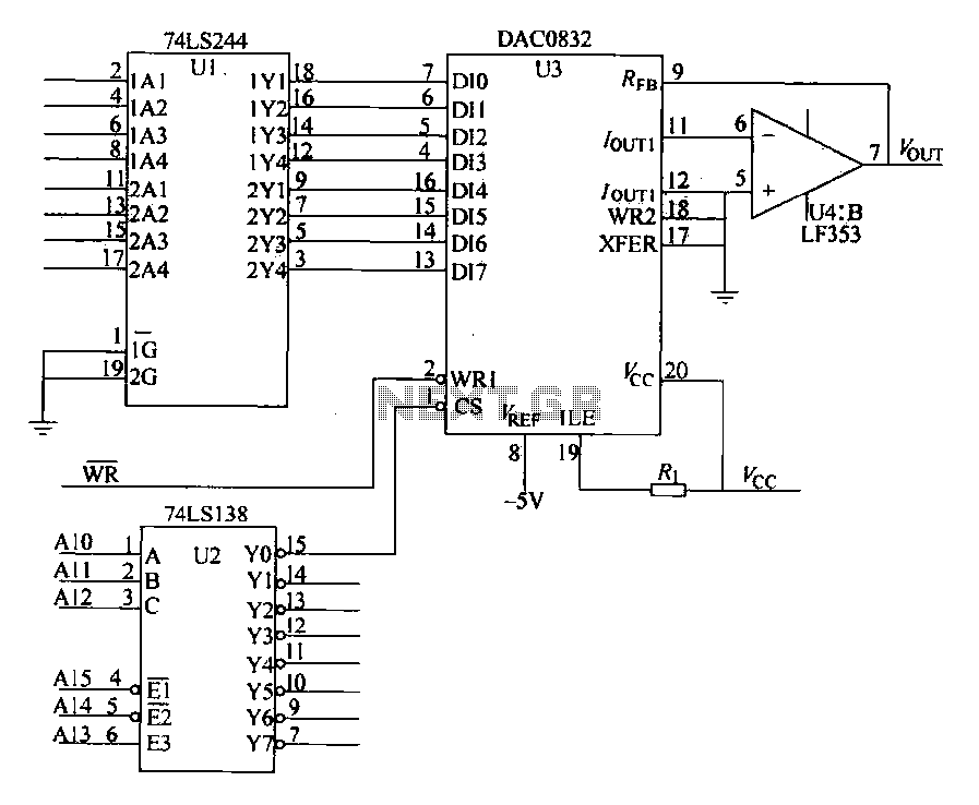
The DAC0832 is depicted in Figure 27-13 as a single-phase circuit connected to the 8086 CPU. The internal 8-bit data input of the DAC0832 must be interfaced with the CPU and the D/A converter interface circuits for data transmission,...