
LCC configuration for Tesla Coil impedance circuit
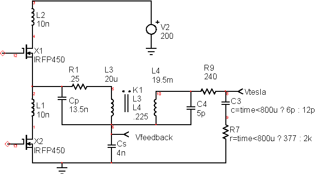
The described Tesla Coil circuit employs an LCC configuration, which optimally balances the energy transfer between the power source and the Tesla Coil. The low coupling coefficient necessitates the careful design of the capacitor network to ensure efficient energy coupling and minimize signal loss due to the primary self-inductance. The series/parallel arrangement of capacitors (Cp and Cs) is critical, as it directly influences the input impedance at resonance, which in turn affects the power transfer efficiency.
In this design, the bridge transistors are capable of handling substantial current and voltage, making them suitable for high-power applications. The strategic use of a boost converter allows for increased output power, demonstrating a flexible approach to managing power levels within the circuit. The careful selection of capacitor values and configurations (10nF and 22nF polypropylene capacitors) ensures that the system can handle the necessary current levels while maintaining operational efficiency.
The introduction of geometric discontinuities in the Tesla Coil antenna is a novel approach to enhancing the electric field strength, which is essential for plasma formation. The use of pyramid-shaped molds is an innovative method to achieve this, potentially increasing the performance of the Tesla Coil. The effects of plasma on circuit behavior, such as increased capacitance and added series resistance, highlight the dynamic nature of the system and the importance of simulation in predicting circuit performance.
The design considerations regarding the operational limits of the MOSFETs are crucial for long-term reliability. By ensuring that the operational current remains within safe limits, the risk of overheating can be minimized, thereby extending the lifespan of the components. The ability to minimize transient stress during switching operations is another significant advantage, contributing to the overall efficiency and reliability of the circuit.
In summary, this Tesla Coil design showcases a sophisticated approach to energy coupling and plasma generation, utilizing advanced circuit configurations and component selection to achieve high performance in a compact form factor. The simulation results provide valuable insights into the circuit's behavior under various conditions, informing further refinements and optimizations.Because the coupling coefficient is so low, the primary self-inductance tends to short out the driving signal. However, if a series/parallel set of capacitors is used to couple energy, then the input impedance will increase at resonance, thus achieving decent power transfer efficiency.
The LCC configuration shown in Figure 14 was chosen to match the Tesla Coil impedance with the half-bridge power capability. The bridge transistors can switch 14 amps at 400 Volts. If the design is setup to output around 250 watts with a 200 Volt input, then an extra boost converter can double the voltage and multiply the power by 4.
The complete Tesla Coil Model with the circuitry using Cp and Cs to couple energy from V2 to Vtesla. If Cp+Cs is made constant, the smaller values of Cs will reduce the required input current, but increase the voltage. That’s how the Tesla Coil is matched to the half bridge capability. When Cs+Cp is reduced, the voltage at Vfeedback will increase and cause greater stress on the capacitors.
If Vtesla is sufficiently large, the air breaks down and plasma streamers will form. The fields near the Tesla Coil can be increased by making geometric discontinuities in the Tesla Coil “antenna.” A pair of pyramid shaped cooking molds were used for this purpose. The plasma will increase the capacitance and add series resistance to the circuit. That affect was simulated by switching the load capacitance and resistance. Cs was formed using 10, 10nf polypropylene capacitors: 2 parallel banks of 5 in series. Cp was formed using 15, 22nf polypropylene capacitors: 3 parallel banks of 5 in series. That furnishes a primary RMS current capability of 2.8 amps; that’s less than the MOSFET capability, so it will be necessary to limit operational time to avoid over heating.
The MOSFET switches can be made to switch on and off with virtually zero transient stress. This is accomplished by adjusting the current phase with respect to the switching voltage. The tuned circuit needs to operate above its resonant frequency for the LCC configuration used. Table 3 shows the simulation results for several values of capacitance with a 100Vac input. 🔗 External reference
Related Circuits
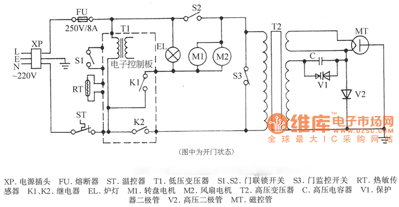
XP power plug, FU fuse, ST temperature control, T1 low-voltage transformers, S1, S2 door interlock switch, S3 threshold control switch, RT thermal sensor, K1, K2 relay, EL furnace light, M1 wheel motor, M2 fan motor, T2 high-voltage transformer, C...
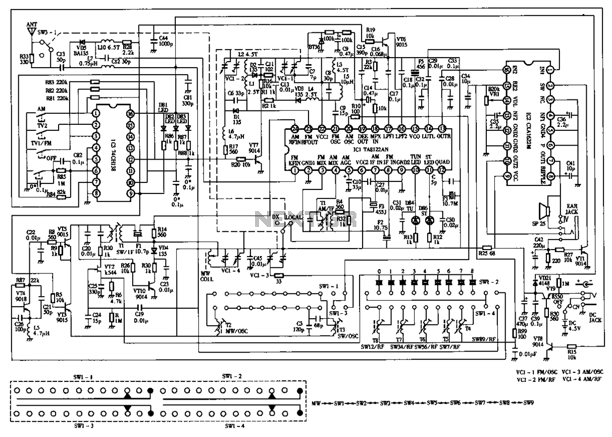
The circuit diagram for the Desheng 119 700 type FM, TV sound, medium wave, and short wave high sensitivity L2-band stereo radio is presented below. The Desheng 119 700 type radio circuit is designed to receive various frequency bands including...
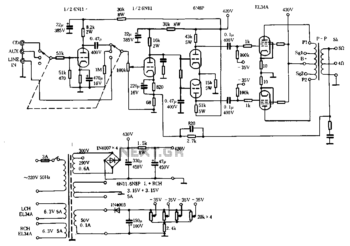
The Ml00 circuit is a typical tube circuit, functioning as a preamplifier. Its input stage utilizes a common cathode amplifier, followed by an inverter stage, culminating in a power amplifier that has been enhanced from a standard connection. This...
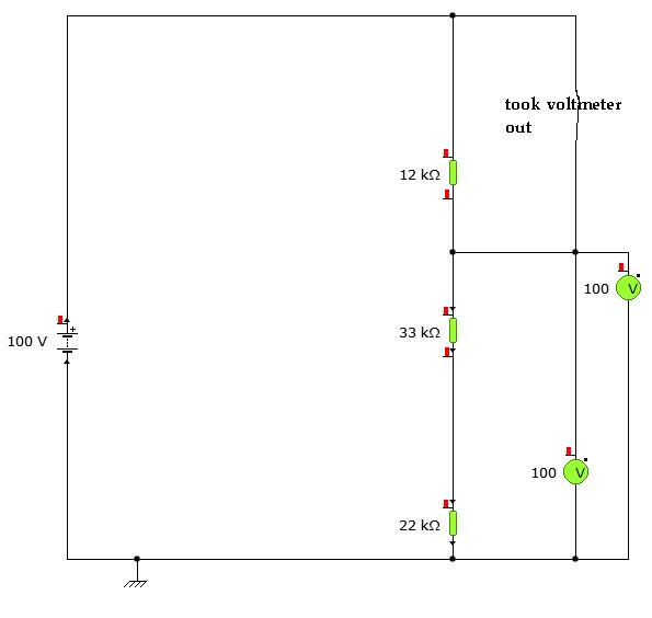
A user is utilizing YENKA software to diagram circuits but is experiencing confusion regarding the voltage calculations in a basic series circuit, as illustrated in the attached image. In a basic series circuit, components are connected end-to-end, forming a single...
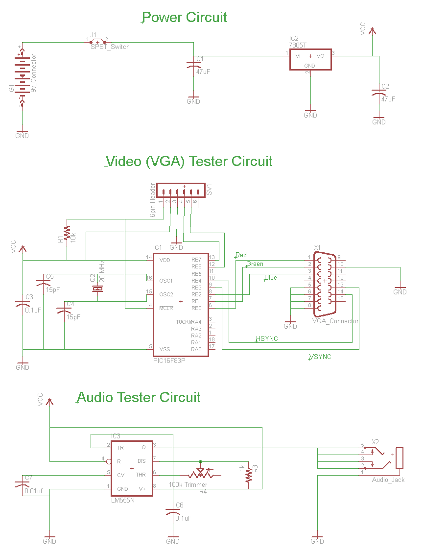
The Mini AV Test Box circuit is designed with simplicity and efficiency in mind. It consists of three main sections, which are clearly delineated in the schematic. The primary components utilized in this circuit include the 7805 voltage regulator,...
Useful for checking diodes, transistors, triacs, SCRs, resistors, and LEDs, this curve tracer should prove beneficial in the experimenter's lab. It displays the volt-ampere characteristic of a two-terminal device on an oscilloscope. This is a simple block diagram of...