
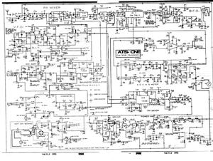
switching power supply circuit diagram

A switching power supply is a type of power supply that uses a switching regulator to convert electrical power efficiently. Unlike linear power supplies, which dissipate excess voltage as heat, switching power supplies operate by rapidly switching the input voltage on and off, allowing for greater efficiency and reduced heat generation.
The basic components of a switching power supply circuit include a transformer, a switching element (such as a MOSFET), a diode, an inductor, and capacitors. The switching element is driven by a pulse-width modulation (PWM) controller, which adjusts the duty cycle of the switching signal to regulate the output voltage.
In a typical schematic, the input voltage is connected to the switching element, which alternates the current flow through the transformer. The transformer steps up or steps down the voltage as required, and the output is rectified by the diode, smoothing the output with capacitors and inductors to reduce ripple voltage. Feedback mechanisms are often incorporated to ensure stable output under varying load conditions, enhancing the reliability of the power supply.
Overall, switching power supply circuits are widely used in various applications due to their compact size, high efficiency, and ability to handle a wide range of input voltages.Welcome folks, today I want post interesting topic about switching power supply circuit diagram for you who want to learn more you can search.. 🔗 External reference
Related Circuits

The circuit was originally available in kit form from a surplus supplier, but it is likely more widely accessible now. It introduces innovative concepts such as utilizing a 555 timer as a pulse width modulator (PWM) and employing serial/parallel...
This example describes the use of HS101 and HS201 radio transmitter and receiver modules to control rotating color lights, functioning as a multi-channel radio remote control device suitable for small dance floors or home use. Users positioned at any...
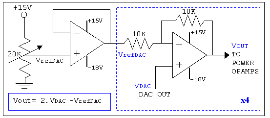
As mentioned in the chapter about the DAC, this circuit shifts the voltage output range. The following diagram explains its operation and structure. The circuit's outputs are connected to the input pins of the power operational amplifiers. The described circuit...
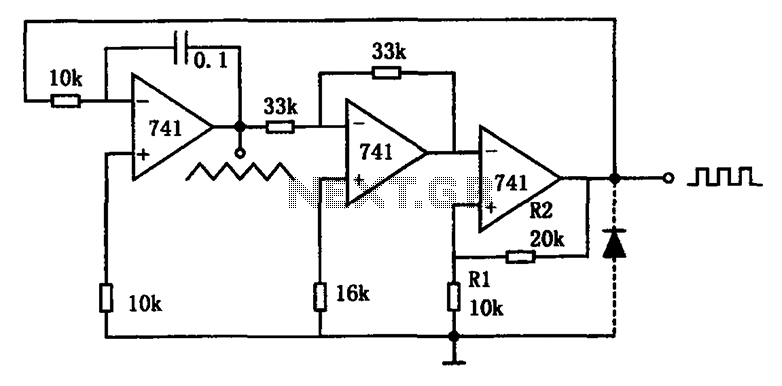
The circuit illustrated generates a variety of low-frequency waveforms, specifically triangle and square waves, simultaneously. It consists of several stages: the first stage is an integrator, followed by a gain stage with an inverter, and a comparator stage that...
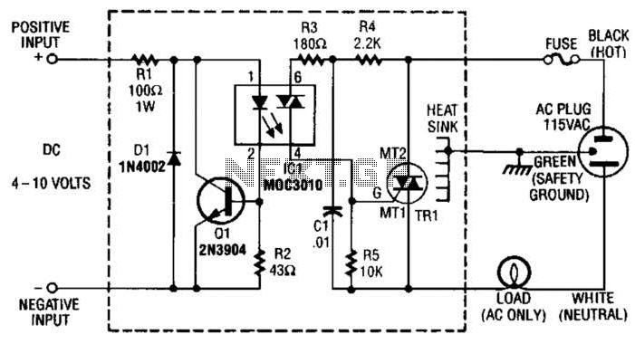
Rl limits input current while Ql acts as a current sink to protect IC1. D1 serves as a polarity protector. IC1 provides a triac output to trigger the main triac, TR1. The circuit consists of several key components that...
The range of this FM transmitter is approximately 100 meters when powered by a 9V DC supply. The circuit consists of three main stages. The first stage is a microphone preamplifier utilizing a BC548 transistor. The second stage features...