
light dependent blinker using ldr and cd4093
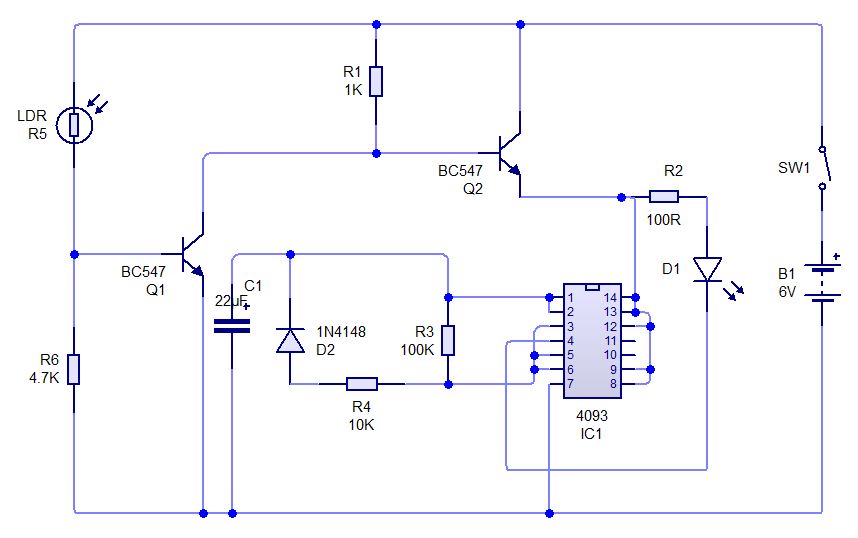
The circuit described utilizes a CD4093, a quad 2-input NAND gate, to create an oscillator that controls the blinking of an LED based on light levels detected by an LDR. The basic principle relies on the behavior of the LDR, which changes its resistance based on the amount of light it receives. When the light is blocked, the resistance of the LDR increases, causing the voltage across it to rise, which activates the transistor Q2 (BC547). This, in turn, powers the CD4093, allowing it to function as an oscillator.
The configuration of the CD4093 as an astable multivibrator is critical for generating the blinking effect. The timing components, R3 and C1, determine the frequency of oscillation. The choice of these components allows for flexibility in adjusting the blinking rate of the LED. The addition of diode D2 ensures that C1 charges quickly, facilitating a rapid response to changes in light levels.
In practical terms, the circuit can be constructed on a mini breadboard, which allows for easy prototyping and adjustments. The LDR should be positioned to receive direct ambient light for the circuit to function correctly. The connections to the CD4093 must be made carefully, ensuring that all unused inputs are tied to the positive rail to avoid unwanted oscillations or floating states. This project serves as an excellent introduction to basic electronics principles, such as light sensing, oscillation, and the use of integrated circuits.Here`s a simple experiment with LDR and CD4093. This is just a modification of a previous project dark sensor using 2 transistors . In this project, the CD4093 is configured in such a way that whenever you block light falling on LDR, the circuit starts blinking the LED D1. The flasher circuit does not get power till there is enough light on LD R. The CD4093 circuit gets power via emitter of Q2- BC547 when you block light falling on LDR. CD4093 is designed as a simple oscillator using its internal NAND gate 1 (comprising input pins 1 and 2 and output pin 3). The oscillator`s external components comprise resistor R3 and capacitor C1. Diode D2 and resistor R4 help in quick charging of capacitor C1. When capacitor C1 charge to around 50% of Vcc, output of gate 1 of CD4093 goes low to discharge capacitor C1.
The output from pin 3 of CD4093 again goes high to charge capacitor C1 again. This cycle repeats and sets up an oscillation (like an astable multivibrator ), which is given to gate 2 (comprising input pins 5 and 6 and output pin 4) of CD4093. Gate 2 serves as a buffer to drive the white LED (D1). For the given values of resistor R3 and capacitor C1, the flashing rate of LED1 is one per second (1 Hz), so, you can put some other values of resistor and capacitor if you want to change the frequency.
Pin 14 of CD4093 is Vcc and all the unused input pins are tied to the positive rail (pin 14) to prevent floating. The circuit can be constructed on a small mini breadboard. HOW TO MAKE PROJECTS ON MINI BREADBOARD Mount LDR such that ambient light falls on it directly and the circuit remains OFF in normal condition.
🔗 External reference
Related Circuits
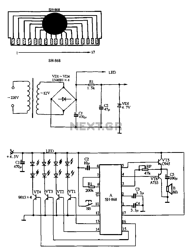
Figure 2-80 illustrates the SH-868, an integrated circuit designed for a music flash circuit powered by three batteries. It can drive a flashing light-emitting diode (LED) while simultaneously activating a sound speaker. The device features a function selection button...
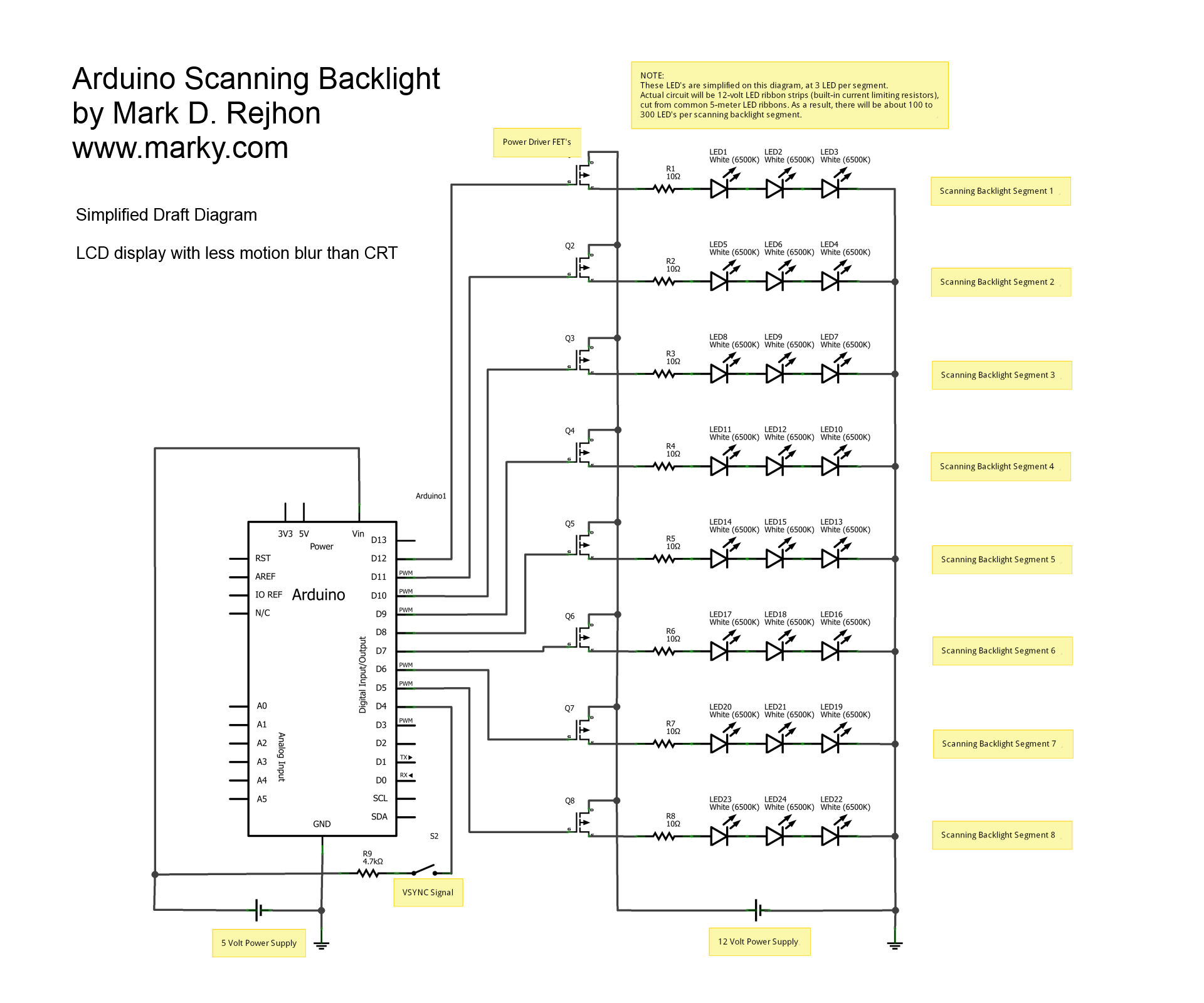
This is a simplified schematic diagram for a homemade scanning backlight driven by an Arduino, an open-source electronics prototyping platform. The Arduino monitors the VSYNC signal (input-lag compensated) and executes a backlight scanning sequence, using ultra-short strobes of super...
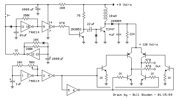
The telephone ring generator described generates the necessary aerial voltage using a simple switched-mode power supply (SMPS). It incorporates a CMOS Schmitt Trigger-based oscillator, a 10 mH inductor, a high-voltage switching transistor (such as the TIP47 or another high-voltage,...
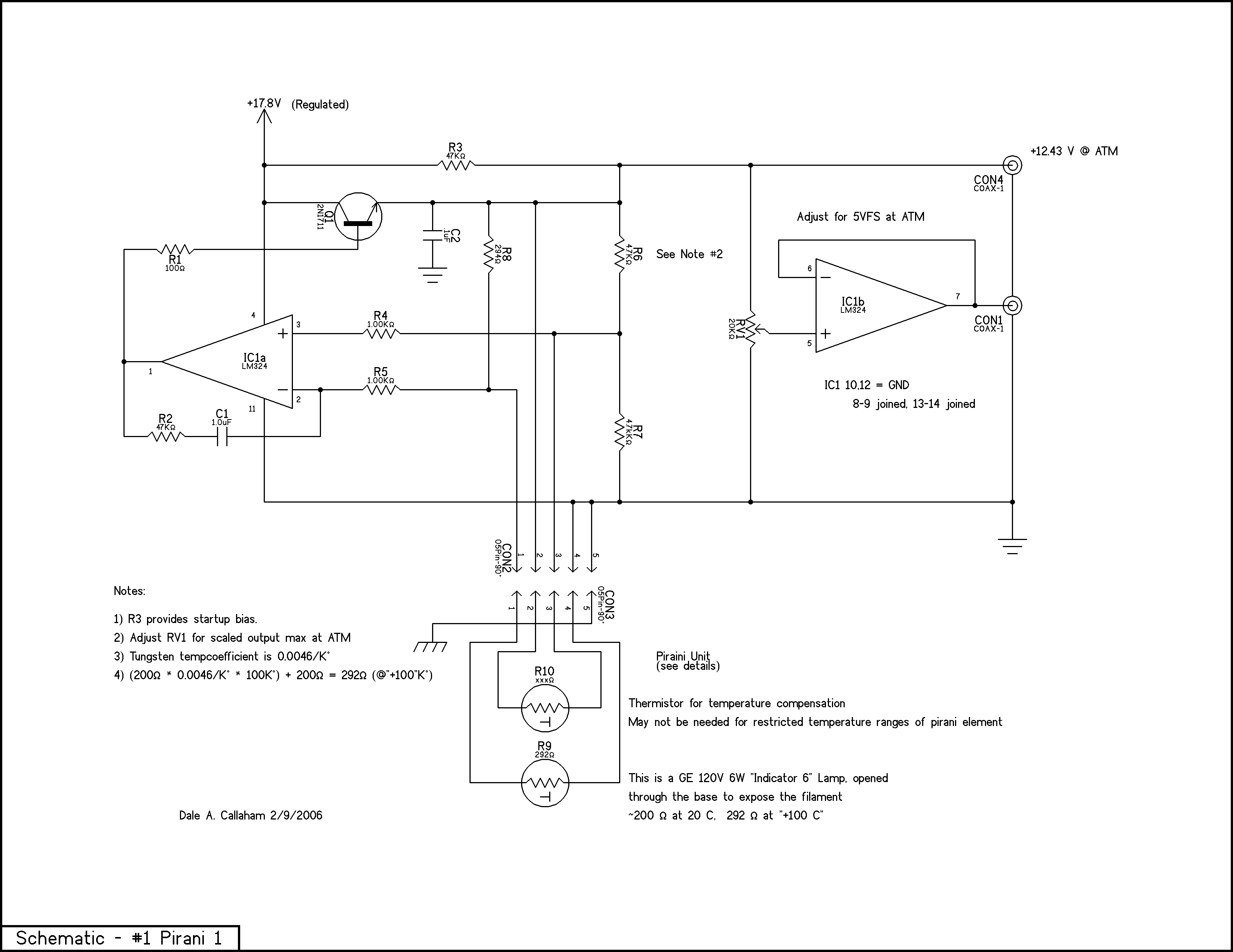
The principle is that the resistance of metals increases at higher temperatures, and a heated wire suspended in a gas will lose heat by conduction and convection in proportion to the number of gas molecules present; thus, the heat...
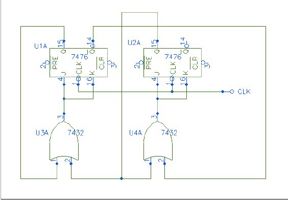
Q1 and Q2 form a table. On the left side, list the four possible states of Q1 and Q2; on the right side, write the values that Q1 and Q2 will assume after the next clock pulse. The table...
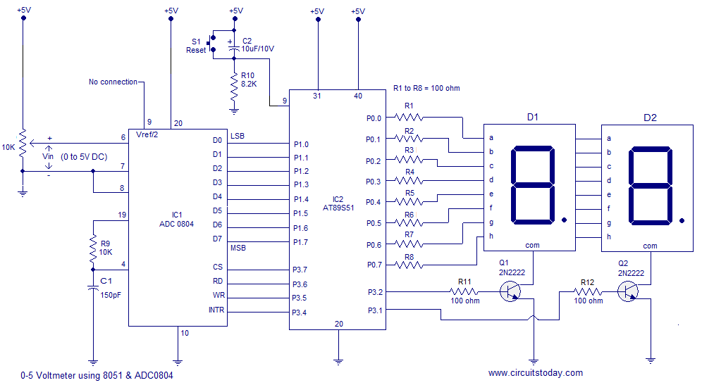
A simple 0-5 digital voltmeter utilizing the 8051 (AT89S51 microcontroller) is presented, accompanied by a circuit diagram and assembly language (ASM) code. This digital voltmeter is designed for straightforward voltage measurement. The circuit employs an AT89S51 microcontroller, which serves as...