
LM12 Simple Power Amplifier
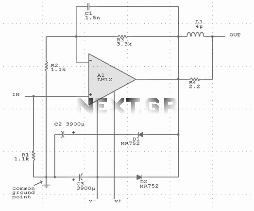
Output-clamp diodes are essential in audio amplifier circuits to protect against voltage spikes generated by inductive loads such as loudspeakers. When the loudspeaker is turned off or when there is a sudden change in the audio signal, the inductive nature of the loudspeaker can generate back EMF (electromotive force), which can potentially damage the amplifier. The output-clamp diodes are placed in parallel with the load to shunt these voltage spikes safely to ground, thereby protecting the amplifier from excessive voltage.
In addition to the output-clamp diodes, output LR (inductor-resistor) isolation is employed to manage load capacitance, which can be as high as 2 mF in audio applications. This isolation is crucial for maintaining audio fidelity and preventing unwanted interactions between the amplifier and the loudspeaker, which can lead to distortion and degradation of sound quality.
Supply-bypass capacitors play a significant role in stabilizing the power supply to the amplifier. These capacitors are typically large and are placed as close to the integrated circuit (IC) as possible. Their primary function is to filter out high-frequency noise from the power supply and to provide a reservoir of charge that can quickly respond to changes in load current. This arrangement prevents the rectified load current from flowing back into the amplifier's supply leads, which can introduce high-frequency distortion and adversely affect audio performance.
Furthermore, implementing a single-point grounding scheme is recommended for all internal leads, as well as for the signal source and load. This approach minimizes the risk of ground loops, which can introduce unwanted noise and distortion into the audio signal. By ensuring that all grounds converge at a single point, the potential for ground loop interference is significantly reduced, thus enhancing the overall audio quality of the amplifier circuit.Output-clamp diodes are mandatory because loudspeakers are inductive loads. Output LR isolation is also used because audio amplifiers are usually expected to handle up to 2 mF load capacitance. Large, supply-bypass capacitors located close to the IC are used so that the rectified load current in the supply leads does not get back into the amplifier, increasing high-frequency distortion.
Single-point grounding for all internal leads plus the signal source and load is recommended to avoid ground loops that can increase distortion. 🔗 External reference
Related Circuits
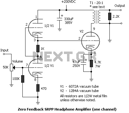
To get a low output impedance I needed to use quite a high step-down ratio (20:1); after all, the amplifier may be used with headphones of lower impedance than the 300 Ohms of the HD600. The output valve is...
In linear equipment design, it is sometimes necessary to take a voltage that is referenced to a certain DC level and generate an amplified output that is also referenced. In linear circuit design, the process of amplifying a voltage that...
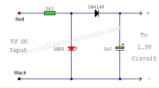
This circuit diagram illustrates a resource replacement for 3V mercury cells or other small batteries. It has various applications, including powering a front panel multi-adapter with a digital thermometer in a computer. The circuit draws power from the PC,...
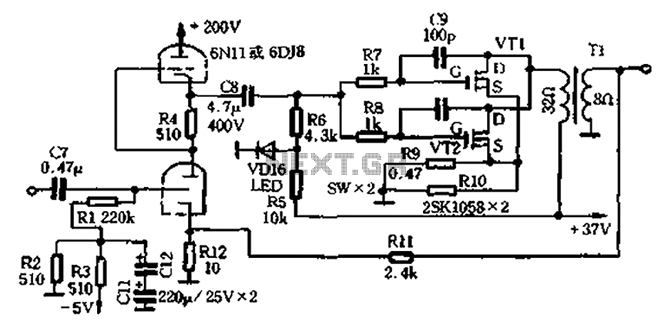
The amplifier circuit illustrated in Figure 2-25 features the following: (1) It utilizes a class 6N11 tube for parallel push-pull amplification, providing high-frequency response and an excellent signal-to-noise ratio. (2) The final stage of the semiconductor amplifier does not...
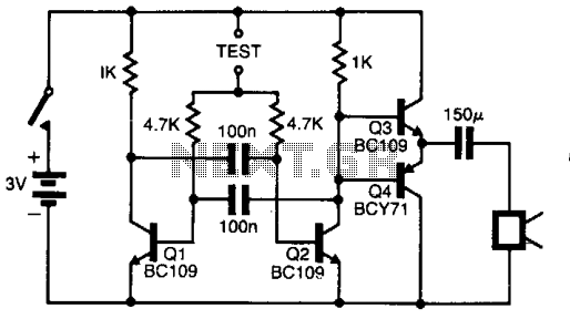
The pitch of the tone is dependent upon the resistance under test. The tester will respond to resistance of hundreds of kilohms, yet it is possible to distinguish differences of just a few tens of ohms in low-resistance circuits....
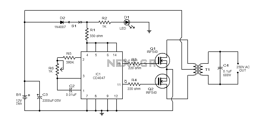
This document provides an explanation of a simple 100-watt inverter circuit using the IC CD4047 and the IRF540 MOSFET. The circuit is designed to be simple, cost-effective, and suitable for assembly on a veroboard. The CD4047 is a low-power...