
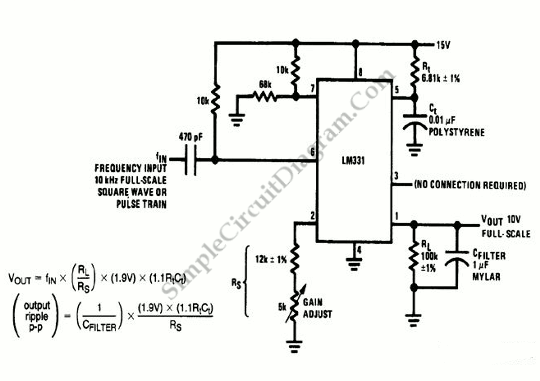
LM331 Frequency to Voltage Converter
The frequency-to-voltage converter circuit is designed to transform frequency signals into a proportional voltage output, making it useful in various applications such as signal processing and measurement systems. The circuit's architecture includes a combination of operational amplifiers, resistors, capacitors, and transistors, which work together to ensure accurate conversion and stable output.
The use of the 741 operational amplifier as a current source allows for precise control over the charging of the timing capacitor (C1), which is critical for maintaining linearity and minimizing distortion in the output signal. The choice of components, including the uni-junction transistor (UJT) and the 555 timer IC, further enhances the circuit's performance by providing stable oscillation and reliable voltage regulation.
In terms of power supply requirements, the circuit operates effectively with dual supply voltages of +5V and -5V, ensuring compatibility with a wide range of input signal levels. The limitation of the input voltage to 0-2V allows for safe operation while still providing adequate output levels for most applications. The ability to adjust gain via a 5 kΩ potentiometer enables users to calibrate the output voltage to match specific requirements, making the circuit versatile for different use cases.
Furthermore, the TMP01 temperature-to-frequency converter showcases the circuit's applicability in temperature sensing and monitoring systems, where analog temperature readings can be transmitted as frequency signals for further processing. The integration of monolithic VFCs in this design not only simplifies the circuit but also enhances reliability and reduces the overall footprint, making it suitable for compact electronic devices.
Overall, this frequency-to-voltage converter circuit exemplifies a well-engineered solution for converting frequency signals into voltage outputs, with a focus on performance, stability, and adaptability across various electronic applications.The frequency to voltage converter circuit illustrated in the schematic diagram below produces a 10 V output for 10 kHz full scale input (square waves or pulses). The simplicity of the circuit doesn`t mean a bad performance: this circuit has linearity about 0. 06% at full scale. For your note, there is a trade-off between ripple versus response tim e. With Cfilter at 1uF, the output ripple is about 13 mV with 0. 6 s settling time. The response time will be quicker if Cfilter is decreased in the expense of increased ripple by the same factor. An increase in Cfilter produces the opposite results. Set the 5Kohm gain adjust for 10 V out with a 10 kHz input to trim. Using this circuit, we can accept positive or negative or differential control voltages. When the control voltage is zero, the output frequency is zero. To charge the timing capacitor C1 linearly, the 741 op amp forms a current source controlled Continue reading †’.
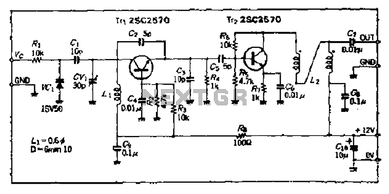
The following voltage to frequency converter (V/FC VCO) circuit consist of a UJT (uni-junction transistor) oscillator in which the timing charge capacitor C2 is linearly depends on the input signal voltage. The voltage across resistor R5 set the charging Continue reading †’. Voltage-to-frequency converter (VFC) circuit is shown in the schematic diagram below. The circuit employs 555 IC as the core of its function. This circuit uses +5V and -5V supply voltages, and the input is limited to 0-2V. You can adjust Continue reading †’. Using this circuit a low voltage battery can be increased to 5V. The need of input voltage of this circuit is only 1. 5V and the output voltage is 5V at 40mA. Using 2. 4V input, this circuit can supply 180mA at Continue reading †’. This is a TMP01 Temperature-to-Frequency Converter circuit. Converting voltage to the frequency domain is another common method of transmitting analog information.
This circuit uses monolithic voltage-to-frequency converters (VFCs) that has some advantages like low cost a robust, and has open-collector Continue reading †’. 🔗 External reference
Related Circuits
The Bong circuit is a high-frequency Colpitts oscillator that utilizes a Ge coil (L). It features two heads and is designed for simple production. The frequency of oscillation can be determined, and testing is conducted to ascertain the value...
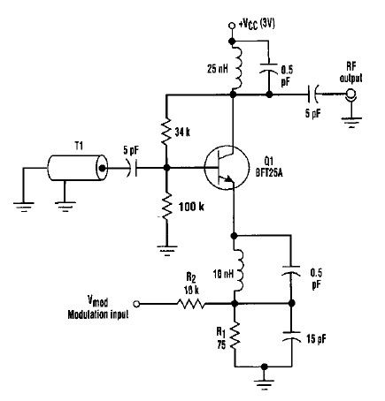
This varactorless high-frequency modulator electronic project must be powered by a simple DC 3-volt power source, such as a 3-volt battery. Traditionally, high-frequency oscillators are frequency-modulated using a varactor. However, varactors typically require a significant voltage change to achieve...
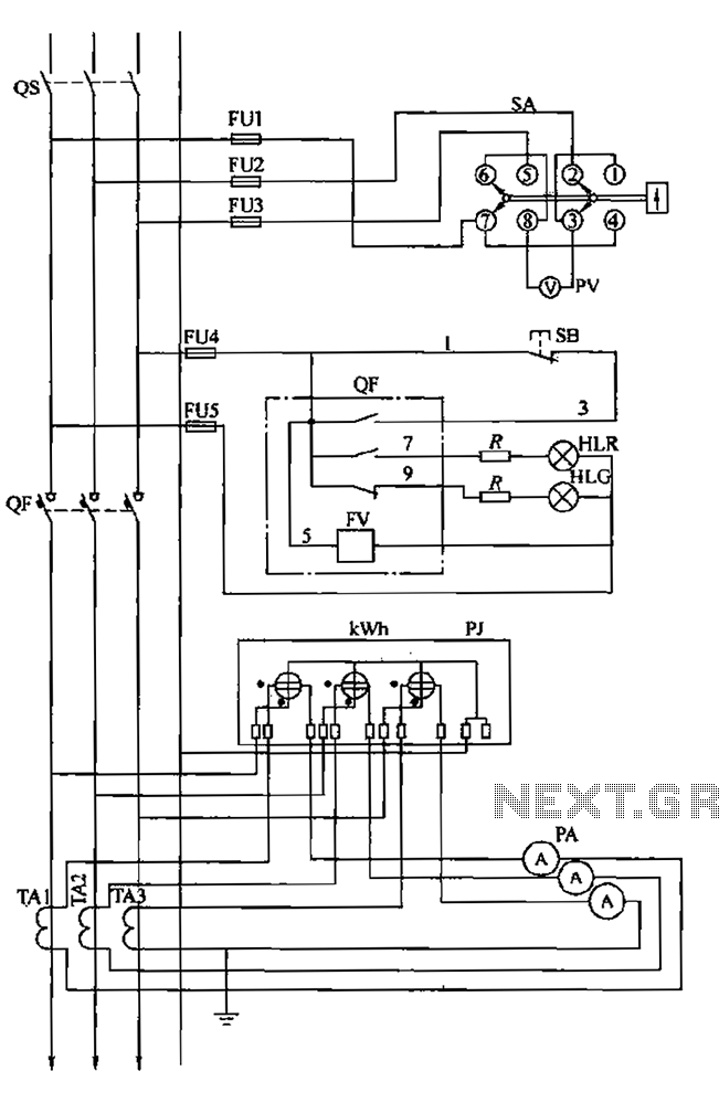
The BSL is illustrated in a low-voltage distribution panel wiring diagram. It consists of three main components: the voltage measuring circuit, secondary circuit protection, and the energy metering circuit. (1) The voltage measuring circuit includes a voltage switch (SA)...
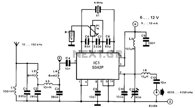
This converter shifts frequencies from 10 kHz to 150 kHz up to 4.01 to 4.15 MHz, suitable for use with a shortwave receiver for very low frequency (VLF) reception. A 4 MHz local oscillator frequency is utilized, and the...

The circuit employs a transistor control mechanism. When the grid voltage is within the normal range, relay KA is activated, supplying power to the load. If the grid voltage falls below the minimum allowable threshold (adjustable via potentiometer RPz)...
The LinkSwitch-XT LNK363DN-based flyback power supply generates a single isolated DC output voltage from an input voltage range of 90 VAC to 264 VAC. The power supply delivers an output of 5 V at 550 mA (2.75 W) in...