
Long duration timer circuit
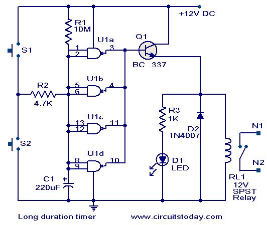
The timer circuit operates on a principle of time delay generated by the combination of resistor R1 and capacitor C1. The timing period is determined by the RC time constant, which is calculated as τ = R1 × C1. In this circuit, the values of R1 and C1 must be selected to achieve the desired delay of approximately 35 minutes. A typical configuration might involve a resistor in the range of several megaohms and a capacitor in the range of microfarads.
Upon pressing switch S2, the circuit initiates the timing sequence. The discharge of capacitor C1 through R1 causes the voltage across C1 to drop. The NAND gates within the CMOS IC 4011 are configured in such a way that when their inputs are at logic low (0V), the outputs transition to logic high, providing the necessary signal to turn on transistor Q1. The transistor acts as a switch for the relay, allowing current to flow through the relay coil, thus energizing the relay contacts and powering the connected device.
The release of switch S2 allows capacitor C1 to charge through R1. As the capacitor charges, the voltage rises until it reaches half of the supply voltage, which is the threshold for the NAND gates. At this point, the outputs of U1 revert to low, turning off transistor Q1 and deactivating the relay. The relay contacts open, disconnecting power from the appliance.
Switch S1 provides a manual override feature, allowing the user to interrupt the timing sequence and turn off the connected device at any point before the timer completes its cycle. This feature enhances user control over the operation of the timer circuit, making it versatile for various applications where automatic shut-off is beneficial.
In summary, this timer circuit effectively combines simple components to create a reliable and energy-saving solution for automatic appliance control. Its design leverages the properties of CMOS technology and passive components to achieve a long time delay, making it suitable for a variety of household and industrial applications.This timer circuit can be used to switch OFF a particular device after around 35 minutes. The circuit can be used to switch OFF devices like radio, TV, fan, pump etc after a preset time of 35 minutes. Such a circuit can surely save a lot of power. The circuit is based on quad 2 input CMOS IC 4011 (U1). The resistor R1 and capacitor C1 produces the required long time delay. When pushbutton switch S2 is pressed, capacitor C1 discharges and input of the four NAND gates are pulled to zero. The four shorted outputs of U1 go high and activate the transistor Q1 to drive the relay. The appliance connected via the relay is switched ON. When S2 is released the C1 starts charging and when the voltage at its positive pin becomes equal to ½ the supply voltage the outputs of U1 becomes zero and the transistor is switched OFF.
This makes the relay deactivated and the appliance connected via the relay is turned OFF. The timer can be made to stop when required by pressing switch S1. 🔗 External reference
Related Circuits

This simple circuit is designed to check transistors, allowing measurements down to 40 ohms across the collector-base or base-emitter junctions. It is also capable of testing output power transistors in amplifier circuits. The circuit operates with a 555 timer...
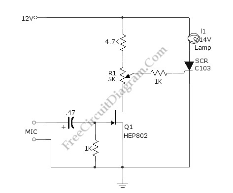
This simple circuit illustrated in the schematic diagram activates the switch using sound. It can be utilized for various applications, such as automatic (sound-controlled) disco lights or car LED light shows. The transistor Q1 amplifies the audio from the...
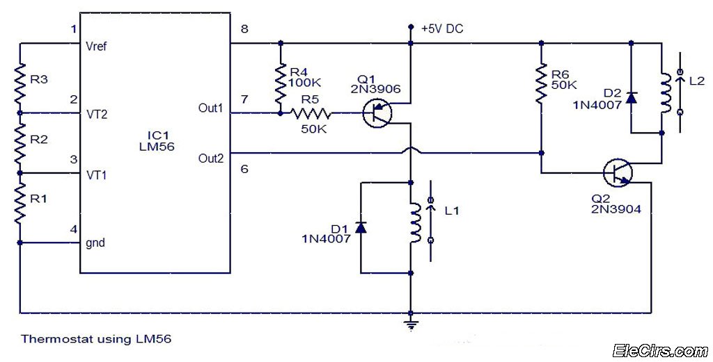
The LM56 Thermostat Project Circuit Diagram includes a schematic for the LM56 thermostat. The values of resistors R1, R2, and R3, which determine the required trip points VT1 and VT2, can be calculated using the following equations: VT1 =...
A second RM output and a sync input have been added to the 555 timer circuit. The sync input is derived from one of Rene Schmitz's voltage-controlled oscillators (VCOs). There are two transistors in the PCB images that lack...
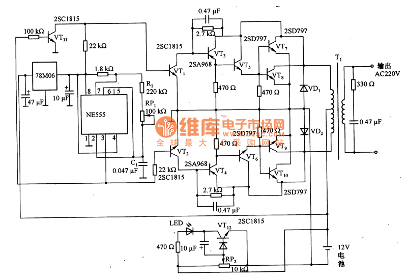
The inverter circuit diagram utilizing the NE555 timer is illustrated, designed to convert a +12V DC battery voltage into a 220V AC output voltage. In this circuit, the NE555 functions as an oscillator, with the oscillation frequency determined by...

The circuit serves as a signal source for calibration level meters or sensor-driven differential transformers. The oscillation frequency is determined by the 74HC04, producing a frequency of 1 kHz through resistor R. The supply voltage of the circuit changes...