
Low Cost Pulse Generator circuit
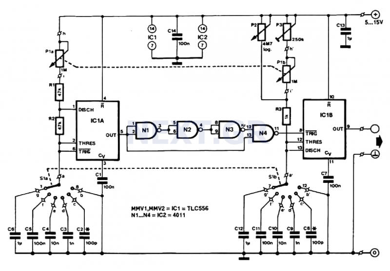
The core of this circuit is the integrated CMOS TLC556, which contains two timing circuits. The first circuit (IC1A) functions as an unstable multivibrator, generating a square wave output at pin 5. The frequency of the output signal can be calculated using the formula:
F = 1 / (In(2) * Cx * (P1a + R1 + 2R2))
The frequency output ranges from 1Hz (with P1a set to 1 MΩ and Cx set to 1 µF) to 100KHz (with P1a set to 0 and Cx set to 100pF). The potentiometers allow for logarithmic frequency variation, where adjusting P1a affects the pulse duration, while the pause duration remains constant. The relationship governing pulse duration is:
Cx * (R1 + R2 + P1a) * In(2)
In contrast, the pause duration is determined by the relationship Cx * R2 * In(2), which is independent of P1a. Connecting the threshold input to ground via switch S1a disables the timeout function.
To mitigate the impact of frequency on the pulse/pause ratio, a delay circuit is implemented using gates N1-N3, which delays and inverts the leading edge. This results in a high level at the inputs of N4 only during the delay period, generating a short trigger pulse.
The second circuit (IC1B) is configured as a monostable multivibrator, where the output frequency depends solely on the trigger pulse frequency. The pulse/pause ratio is adjustable via potentiometer P2. Additional components P1b, P3, R3, and capacitors C8-C12 limit the maximum pulse duration of the monostable multivibrator to ensure it does not exceed the time constant of IC1A.
Construction of the pulse generator is straightforward, allowing assembly on a perforated board if a printed circuit board is not desired. Proper wiring is crucial for functionality. The output pulse can be calibrated using an oscilloscope, ensuring IC1B triggers correctly. It is important to use appropriate capacitor values (C2 and C8) to avoid issues with internal parasitic capacitances of the integrated circuits.
The pulse generator can be powered by a 9V battery or a regulated power supply ranging from 5-15V, such as an LM317. The circuit consumes approximately 0.3mA at 9V, and the output signal amplitude corresponds to the supply voltage. For TTL circuits, a 5V supply is recommended, while CMOS circuits should match the supply voltage of the integrated CMOS. The generator can output a maximum current of 10mA at a high logic level and can sink up to 100mA at a low logic level.
List of Components:
Resistors:
1. R1, R2 = 47KΩ
2. R3 = 1KΩ
3. P1 = 1MΩ stereo potentiometer
4. P2 = 4.7MΩ logarithmic potentiometer
5. P3 = 250KΩ trimmer potentiometer
Capacitors:
1. C1, C5, C7, C11, C14 = 100nF
2. C2, C8 = 100pF Styroflex
3. C3, C9 = 1nF
4. C4, C10 = 10nF
5. C6, C12, C13 = 1µF MKT
Semiconductors:
1. IC1 = TLC 556
2. LC2 = 4011 or CD4011BE or HCF40118E
Miscellaneous:
1. S1 = rotary switch 2x6
2. BNC plug
3. Single-pole switchThis pulse generator produces square pulses from 1Hz to 100KHz with adjustable pulse width of nearly 0-100%. The generator is powered with a voltage of 5-15V and is therefore suitable for both TTL and CMOS circuits.
If you want to measure the response of an amplifier or give timing pulses to a variable frequency digital circuit or drive a pulse width control circuit or if you just want to experiment, you may need a pulse generator.
Dual timing circuit
The most important part of its circuitry is the integrated CMOS TLC556 that incorporates two integrated timing circuits. In the Figure, you see the general diagram of such an integrated and the pin assembly of the single 555 and the double 556.
The ICIA is connected as an unstable multivibrator and generates a square signal at its output (pin 5).
The frequency is given by the formula:
F = 1 / In2 • Cx (P1a + R1 + 2R2)
And depends on the placement of S1a and P1a.
Thus, we have output frequencies of 1Hz (P1a = 1 MΩ, Cx = 1 μF) up to 100KHz (P1a = O, Cx = 100pF).
Each potentiometer implies a frequency variation in a logarithmic ten region. Each change in frequency also implies a change in pulse rate to pause. By shifting the potentiometer to its maximum resistance value, the pulse duration is extended to ten times while the pause duration remains unchanged.
This is explained by the fact that the pulse duration depends on the relationship:
Cx (R1 + R2 + P1a) In2
And hence from the position of the potentiometer, while the pause duration is dependent on the Cx.R2 In2 relationship and is of course independent of P1a. If you connect the Threshold input via ground to S1a, the timeout is turned off.
To neutralize the effect of the frequency on the pulse / pause ratio of the output we still need a time which will be triggered by a rising edge at the spike 5.
The chain of the gate N1-N3 delays and reverses the front Thus, at the entrances of N4 we can We have a high level only during the delay of the front through N1-N3 and thus only until the trigger pulse of LC b. In the drawing you can see the temporal correlation of the signals: The rising pulse front at N4 spike 13, the delayed and inverted front at spike 12 (waist) and the coincidence of the two signals that gives us the short trigger pulse at the spike 11 (below).
IC1B, unlike IC1A, is connected as a monostable multivibrator.
The frequency of the output signal is only dependent on the frequency of the trigger pulse. While the pulse / pause ratio depends only on the position of the P2 rotor. However, via P1b, P3, R3 and C8-C12 a necessary limitation is imposed on the maximum pulse duration of the manostable multivibrator so that it never exceeds the P1α / C2-C6 time constant of IC1A. In the drawings you see square output signals with different pulse / pause ratios.
Construction
The construction is so simple that it can also be done on a perforated board if you do not want to design the printed one.
If you do not make mistakes in the wiring, then the circuit can only work. With the oscilloscope you will set the P3 (P2 to its maximum value) so that the output pulse is just below the period at the IC1A output. This will make sure that IC1B is properly triggered
But add something for C2 and C8. If charging and discharging times are very small then we have an effect of the internal parasitic capacities of the integrated ones.
To precisely observe the logarithmic tens of frequency, you must necessarily experiment by lowering the C2 and C8.
The pulse generator can be powered either by a 9V battery or by a fixed adjustable 5-15V power supply perhaps using an LM317. The circuit consumes approximately 0.3mA at 9V. The amplitude of the output signal is practically the same as the supply voltage of the pulse generator.
So for TTL circuits you will feed with 5V while for CMOS circuits you will supply the generator with a voltage equal to the supply voltage of the integrated CMOS. The generator provides a maximum current of 10mA when the output level is high (logic 1) and can receive a current of 100mA when the output level is low (logic 0).
List of Components
Resistors
- R1, R2 = 47KΩ
- R3 = 1KΩ
- P1 = 1MΩ stereo potentiometer
- P2 = 4M7 logarithmic potentiometer
- P3 = 250KΩ trimmer potentiometer
Capacitors
- C1, C5, C7, C11, C14 = 100n
- C2, C8 = 100p Styroflex
- C3, C9 = 1n
- C4, C10 = 10n;
- C6, C12, C13 = 1m MKT
Semiconductors
- IC1 = TLC 556
- LC2 = 4011 or CD4011BE or HCF40118E
Difference
- S1 = rotary switch 2x6
- BNC plug
- Single-pole switch
Related Circuits

This circuit detects a missing pulse or an abnormally long interval between consecutive pulses in a pulse train. The timer is configured in monostable mode, with the time delay set slightly longer than the duration of the input pulses....
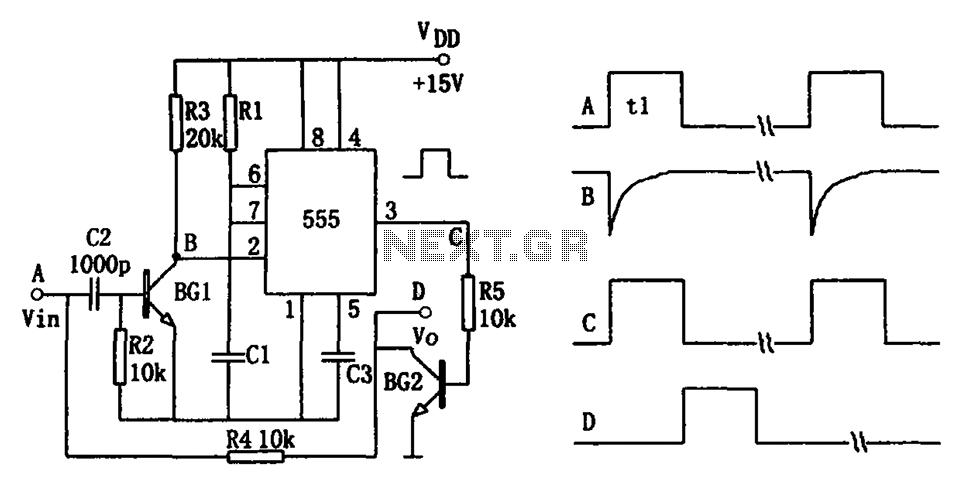
The pulse-width detection circuit is illustrated in the figure and consists of a differential circuit (R2, C2), an amplifier (BG1), a single stabilizing circuit (555, R1, C1), and various other components. The pulse signal Vin (depicted as waveform A)...
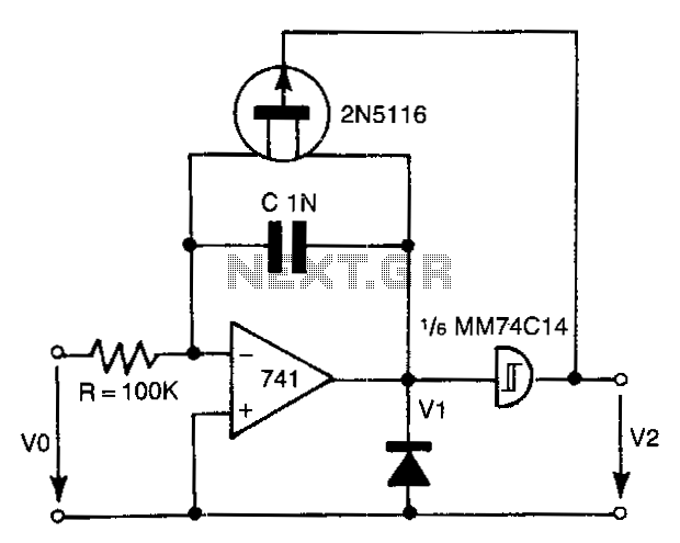
The 741 operational amplifier integrator signal is input into the Schmitt trigger of an inverter. When the signal reaches the positive-going threshold voltage, the inverter's output switches to zero. This output directly controls the FET switch. With a gate...
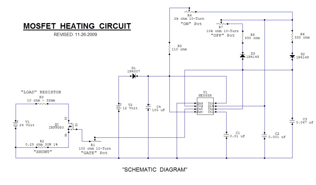
This open-source thread focuses on the development of a "MOSFET Heating Circuit," which is a modified version of an existing design. The MOSFET Heating Circuit is designed to efficiently manage and control heating elements using MOSFET technology. MOSFETs (Metal-Oxide-Semiconductor Field-Effect...
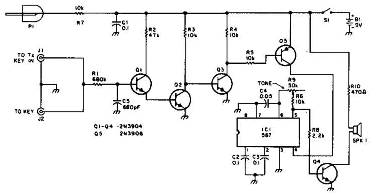
For use with low-power transmitters that require a positive keying voltage. The transistors Q1, Q2, and Q3 are configured as a switching amplifier. When the key is pressed, the collector of Q3 is pulled to ground, which activates Q5...
Access to the resistors was available, and measurements indicated an open circuit when disconnected from any ground or input source. The circuit in question involves resistors that have been verified for accessibility. When measured in isolation—meaning they are not connected...