
Low-Frequency Crystal Oscillator Circuit
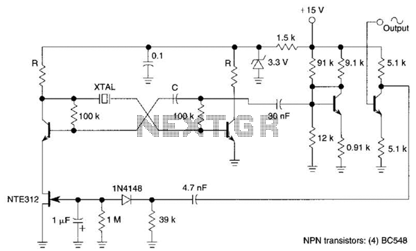
The described circuit employs a modified astable multivibrator configuration using transistors Q1 and Q2 to generate oscillations. The automatic adjustment of the loop gain to the oscillation threshold is facilitated by field effect transistor Q3, which plays a critical role in maintaining stable oscillation conditions. This automatic gain control ensures that the circuit remains operational across varying load conditions and environmental factors.
Transistor Q4 serves as a linear amplifier, taking the output signal from the collector of Q2. Its primary function is to amplify the oscillatory signal while also providing isolation between the oscillator and the subsequent output stage. This isolation is essential to prevent feedback that could destabilize the oscillator. The output from Q4 is characterized by a clean sine wave with an amplitude of 2.5 V, making it suitable for driving resistive loads of 20 kΩ or higher. The wideband operation of this stage indicates that the circuit can effectively handle a range of frequencies without significant distortion, which is crucial for applications requiring high fidelity in signal reproduction.
The inclusion of transistor Q5, which operates with a voltage gain of 1, ensures that the output is not influenced by the nonlinear characteristics of rectifier D1. This isolation is important as it preserves the integrity of the output signal, allowing for accurate signal processing downstream without introducing unwanted distortions from the rectification process. Overall, the circuit is designed to provide reliable oscillation, effective amplification, and signal integrity, making it suitable for various electronic applications. Ql, Q2, and the associated circuitry form a modified astable multivibrator in which the loop gain is automatically adjusted to the threshold of oscillation by means of field effect transistor Q3. Q4 linearly amplifies the signal present at the collector of Q2 and isolates the oscillator section of the circuit from the output.
This stage features wideband operation and delivers a clean 2.5-V amplitude sine wave into a resistive load greater than or equal to 20 kQ. The stage comprising Q5 has a voltage gain of 1 and its sole purpose is to isolate the nonlinear effects of rectifier D1 from the output. 🔗 External reference
Related Circuits
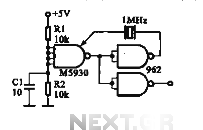
A crystal oscillator is implemented using a DTL (Diode-Transistor Logic) integrated circuit. The oscillation frequencies are 100 kHz and 1 MHz. The circuit consists of a gate circuit that generates a signal for the oscillator circuitry in DTL. The crystal...
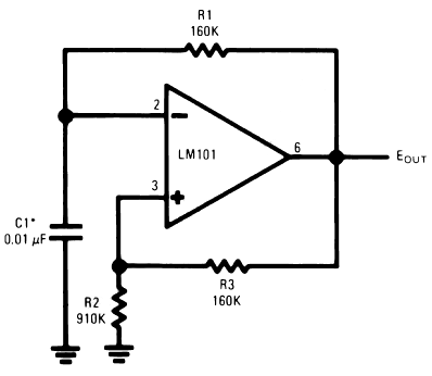
The timing capacitor (C1) generates multiple time constants, facilitating substantial voltage fluctuations at the input, attributable to the LM101's extensive input voltage range. It is advisable to decrease the value of resistor R2 and to increase the capacitance of...
How the processor produces 3 as the output. This question may be challenging to answer in simple terms. If so, a link to a book would be helpful. The process by which a processor generates the output of the number...
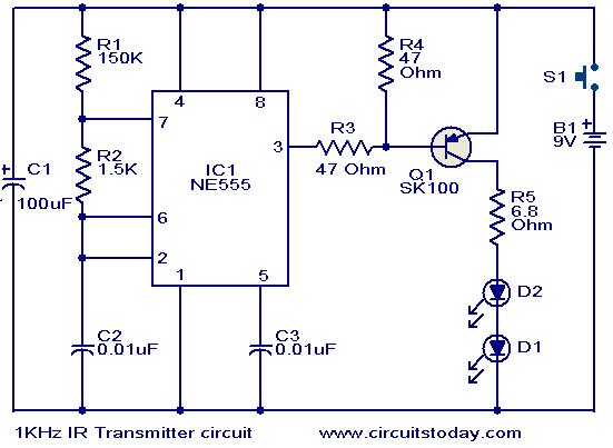
This circuit was designed in response to a request for a 1 kHz infrared (IR) transmitter circuit suitable for remote control applications. It is intended to serve as a low-power IR transmitter with an operating frequency of 1 kHz,...
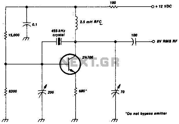
This crystal-oscillator circuit utilizes a 455-kHz crystal. It is a straightforward project. The crystal oscillator circuit based on a 455-kHz crystal operates by utilizing the piezoelectric properties of the crystal to generate a stable frequency. The circuit typically consists of...
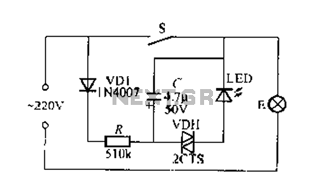
Figure 2 illustrates a circuit for a flashing light switch indicator. When switch S is closed, the normal light E illuminates, while the flashing light indicates a power loss when the system is not operational. When switch S is...
Warning: include(partials/cookie-banner.php): Failed to open stream: Permission denied in /var/www/html/nextgr/view-circuit.php on line 713
Warning: include(): Failed opening 'partials/cookie-banner.php' for inclusion (include_path='.:/usr/share/php') in /var/www/html/nextgr/view-circuit.php on line 713