
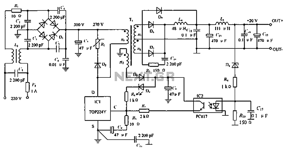
Low Loss Step Down Converter
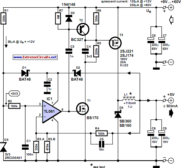
The circuit employs a buck converter topology, which is adept at stepping down voltage efficiently. The use of a high-quality power MOSFET ensures minimal conduction losses, while the feedback mechanism involving IC1 maintains the output voltage stability. The switching action of T1 and T3 is crucial for energy transfer from the input to the output, and the inclusion of capacitors C3 and C4 aids in managing transient responses and improving overall efficiency. The design's adaptability to various input voltages makes it suitable for diverse applications in solar energy systems, particularly where low power consumption is essential. The careful selection of components, particularly in terms of their electrical characteristics, underpins the circuit's performance and operational longevity.This circuit arose from the need of the author to provide a 5 V output from the 24 V battery of a solar powered generator. Although solar power is essentially free it is important not to be wasteful especially for small installations; if the battery runs flat at midnight you`ve got a long wait before the sun comes up again.
The basic requirement w as to make an efficient step-down converter to power low voltage equipment; the final design shown here accepts a wide input voltage from 9 to 60 V with an output current of 500 mA. The efficiency is very good even with a load of 1 mA the design is still better than a standard linear regulator.
The low quiescent current (200 µA) also plays a part in reducing losses. Some of the components specified (particularly the power MOSFET) are not the most economical on the market but they have been deliberately selected with efficiency in mind. When power is applied to the circuit a reference voltage is produced on one side of R2. D1 connects this to the supply (pin 7) of IC1 to provide power at start-up. Once the circuit begins switching and the output voltage rises to 5 V, D2 becomes forward biased and powers the IC from the output.
Diode D1 becomes reverse biased reducing current hrough R1. When the circuit is first powered up the voltage on pin 2 of IC1 is below the reference voltage on pin 3, this produces a high level on output pin 6. The low power MOSFET T1 is switched on which in turn switches the power MOSFET T3 via R5 and the speed-up capacitor C4, the output voltage starts to rise.
When the output approaches 5 V the voltage fed back to the inverting input of IC1 becomes positive with respect to the non inverting input (reference) and switches the output of IC1 low. T1 and T3 now switch off and C3 transfers this negative going edge to the base of T2 which conducts and effectively shorts out the gate capacitance of T3 thereby improving its switch off time.
The switching frequency is not governed by a fixed clock signal but instead by the load current; with no load attached the circuit oscillates at about 40 Hz while at 500 mA it runs at approximately 5 kHz. The variable clock rate dictates that the output inductor L1 needs to have the relatively high value of 100 mH.
The coil can be wound on ferrite core material with a high AL value to allow the smallest number of turns and produce the lowest possible resistance. Ready-made coils of this value often have a resistance greater than 1R and these would only be suitable for an output load current of less than 100 mA.
The voltage divider ratio formed by R4 and R3 sets the output voltage and these values can be changed if a different output voltage is required. The output voltage must be a minimum of 1 V below the input voltage and the output has a minimum value of 4 V because of the supply to IC1.
A maximum efficiency of around 90 % was achieved with this circuit using an input voltage between 9 and 15 V and supplying a current greater than 5 mA, even with an input voltage of 30 V the circuit efficiency was around 80 %. If the circuit is used with a relatively low input voltage efficiency gains can be made by replacing D4 with a similar device with a lower reverse breakdown voltage rating, these devices tend to have a smaller forward voltage drop which reduces losses in the diode at high currents.
At higher input voltage levels the value of resistor R1 can be increased proportionally to reduce the quiescent current even further. 🔗 External reference
Related Circuits

Stepper motor control circuit diagram using TLE5206 for remote control car. The stepper motor control circuit is designed to manage the operation of a stepper motor, specifically utilizing the TLE5206 integrated circuit. This circuit is particularly suitable for applications in...
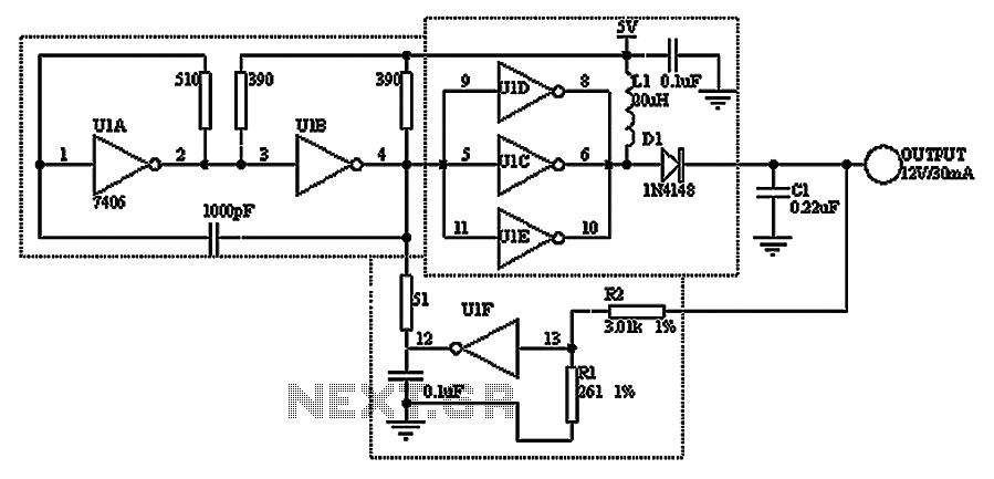
A TTL hex inverter circuit can function as a DC/DC converter, converting 5V to 12V. This circuit encompasses all necessary functionalities for DC/DC conversion. It relies on a TTL switching threshold voltage regulator. The components U1A and U1B form...
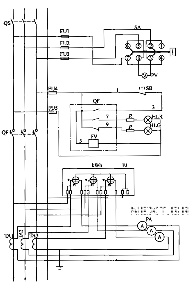
The BSL is illustrated in a low-voltage distribution panel wiring diagram. It consists of three main components: the voltage measuring circuit, secondary circuit protection, and the energy metering circuit. (1) The voltage measuring circuit includes a voltage switch (SA)...
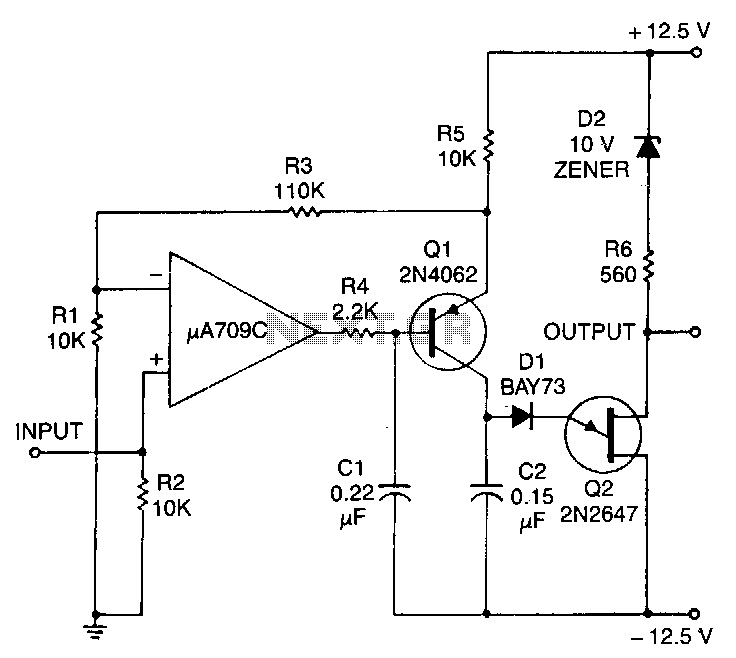
This circuit consists of a UJT oscillator where the timing charge capacitor C2 is linearly dependent on the input signal voltage. The charging current is determined by the voltage across resistor R5, which is precisely controlled by the amplifier....
The circuit depicted in the figure is designed to achieve a higher power output by modifying specific components. On the left side of the figure, components R1, L1, D1, and capacitors C1 to C7 form a conventional filtering and...

A low-cost solution for charging both NiCd and NiMH batteries is presented. The circuit diagram illustrates a universal charger designed for these battery types. The circuit for the low-cost universal charger for NiCd and NiMH batteries typically incorporates several key...