
LPF circuit for rear fill decode
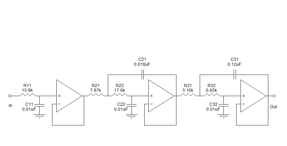
The schematic in question incorporates operational amplifiers, which are essential components in various analog signal processing applications. The triangular symbols in the diagram denote these op-amps, which can amplify voltage signals, perform filtering functions, and serve as building blocks for more complex circuits. When selecting op-amps, it is advisable to choose generic models that meet the required specifications for the intended application.
The circuit's design assumes a split power supply, typically providing both positive and negative voltage rails (e.g., +15V and -15V). This configuration is crucial for op-amps to function correctly, especially when dealing with AC signals that oscillate around a zero-volt reference. If a split power supply is unavailable, a virtual ground can be created using a single power supply, but this may limit the op-amp's performance.
The schematic is noted to be simplified, which may omit several critical components necessary for reliable operation. For instance, bypass capacitors should be included on the power supply lines to filter out noise and stabilize the voltage supplied to the op-amps. These capacitors are typically placed close to the power pins of the op-amps to reduce the effects of inductance in the power supply traces.
Furthermore, a coupling capacitor should be added at the input of the op-amp stage. This capacitor serves to block any DC offset from the input signal, allowing only the AC component to pass through. This is particularly important in filter applications, where the goal is to isolate specific frequency ranges while eliminating unwanted DC levels.
In summary, while the schematic provides a foundational understanding, it requires further refinement and additional components to ensure proper functionality and reliability in practical applications. Careful consideration of the power supply configuration, as well as the inclusion of bypass and coupling capacitors, will enhance the overall performance of the circuit.Need a little help getting this schematic figured out, most of it is understood with the exception of the triangular objects(amps-opamps?) Not sure what those are or how to implement and order them. Here is the diagram thus far(planning to test with a lpf at 1k and 500, with the hpf staying around 80-100hz)
The triangle things are opamps, any generic part would do. But the circuit assumes a split +/- power supply which you don't have. It's also much simplified and not detailed enough to be practical. A real circuit would have bypass caps on the power supplies and a coupling cap at the input etc. 🔗 External reference
Related Circuits
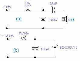
These two circuits are interesting from an academic point of view. Their practical implementation is rather critical and it is not easy to get steady operation. Circuit (a) requires a "cooked" zener: connect it first to a constant current...
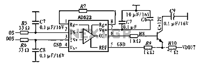
The AD623 is an integrated 3-way amplifier that can operate with either a single or dual supply. It features high common-mode rejection ratio (CMRR) and low voltage drift, along with programmable gain control via an external resistor. All components...
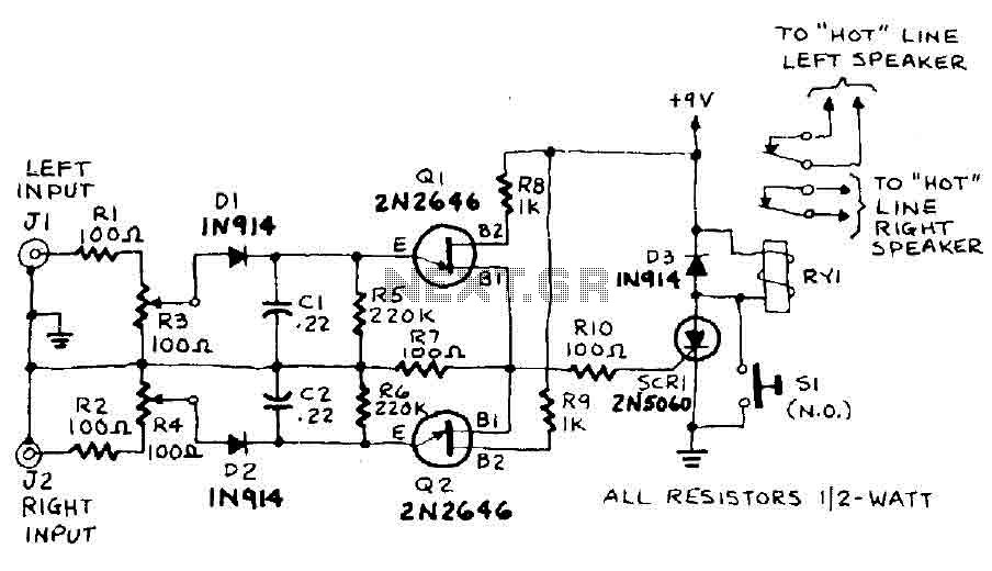
The circuit input is derived from the terminal loudspeaker or amplifier output jacks. If the right channel signal is sufficiently strong to charge capacitor C1 to a potential that exceeds the breakdown voltage of the emitter of transistor Q1,...
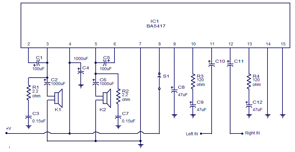
The BA5417 is a stereo amplifier integrated circuit (IC) that features several advantageous characteristics, including thermal shutdown, a standby function, soft clipping, and a wide operating voltage range. It can deliver 5 watts per channel into 4-ohm loudspeakers when...
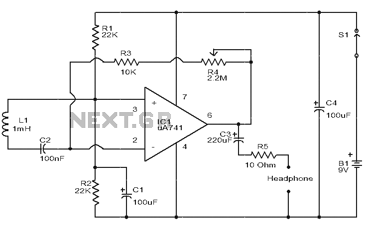
This is a simple circuit designed to detect electromagnetic radiation, including hidden wiring. It utilizes a 1mH inductor to sense the electric field. The induced voltage from the inductor is amplified by an operational amplifier (op-amp). An audio headset...
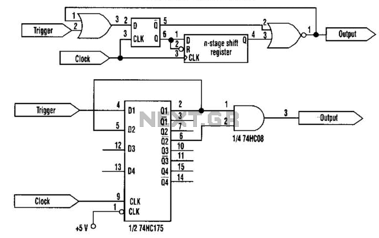
This approach utilizes a Hip-Hop, a shift register, and two gates (A). Before the one-shot pulse, the output of the NOR gate is 0. Consequently, the data input of the D-type flip-flop is equivalent to the trigger. When a...