
MAX4685 circuit and input current limit resistors
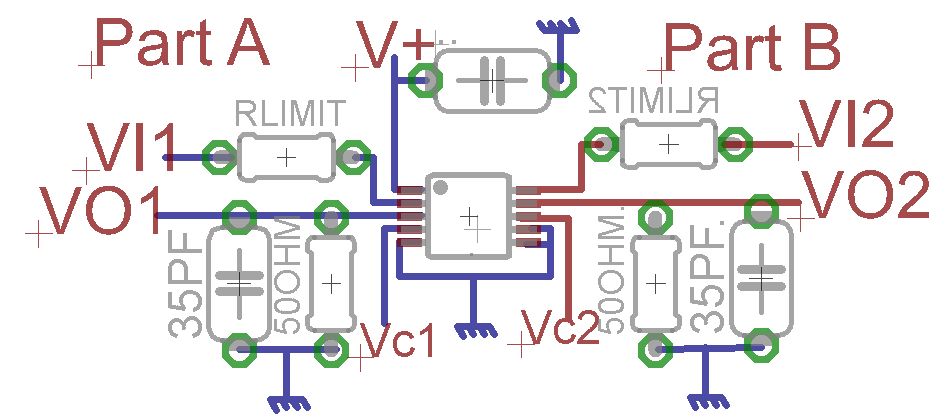
The MAX4685 is a low-voltage, dual analog switch designed for low on-resistance and high-speed switching applications. In a typical configuration, the device can be used to connect either of the two inputs, VI1 or VI2, to a common output.
For the connection diagram, it is essential to identify the pins of the MAX4685. The device features a total of 8 pins, with the following key pin functions:
1. **V+ (Pin 1)**: This pin is connected to the positive supply voltage, typically ranging from 2.7V to 12V.
2. **GND (Pin 4)**: This pin is connected to the ground of the circuit.
3. **IN1 (Pin 2)**: This pin is the control input for switch S1, determining whether VI1 is connected to the output.
4. **IN2 (Pin 3)**: This pin is the control input for switch S2, determining whether VI2 is connected to the output.
5. **COM (Pin 5)**: This is the common output pin where the selected input (either VI1 or VI2) will be directed.
6. **NO (Pin 6)**: This pin connects to the normally open terminal of switch S1.
7. **NC (Pin 7)**: This pin connects to the normally closed terminal of switch S1.
8. **GND (Pin 8)**: This serves as an additional ground reference.
To implement the switching functionality, the control inputs IN1 and IN2 should be driven high or low, depending on the desired connection. When IN1 is high, VI1 is connected to COM, while IN2 being high connects VI2 to COM. It is crucial to ensure that both control inputs are not activated simultaneously to avoid short-circuiting the supply.
The circuit design should also include bypass capacitors close to the V+ and GND pins to filter out noise and ensure stable operation. Additionally, proper consideration must be given to the load connected to the COM pin, as excessive current may exceed the switch's ratings, leading to potential damage.
In summary, the MAX4685 analog switch can effectively manage the connection between two input signals and a common output, allowing for versatile signal routing in various electronic applications. Proper attention to the control logic and electrical characteristics will ensure reliable performance in the intended application.Dear friends i need your advice about the connection diagram of the MAX4685 analog switch attached. I have two inputs VI1 and VI2 and hence we have.. 🔗 External reference
Related Circuits
This scan is from an old ETI Circuits #2 publication from the 1970s. It contains valuable operational amplifier information that is highly useful. With some knowledge, the six circuits presented serve as an instant reference, enabling various applications. These...
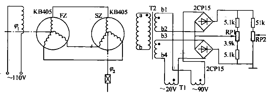
The transmitter (FZ) winding and receiver (SZ) correspond to the three-phase windings connected to a 110V AC voltage supply for transmission. The field winding, early start angle, and receiver output voltage at both ends of the stator windings reflect...
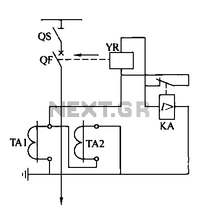
Operating power protection devices can be categorized into two types: DC power supply operation and AC operation. AC operating power is favored due to its lower investment costs, simpler operation, and reliable secondary circuit maintenance, making it widely used...
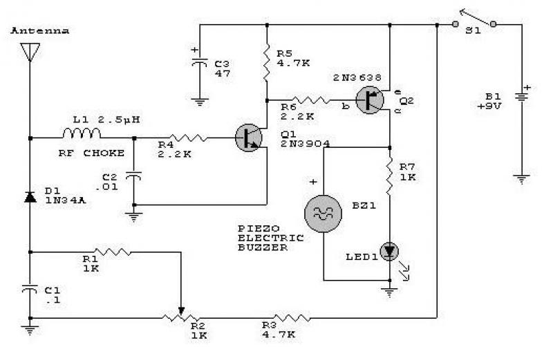
This circuit responds to RF signals below the standard broadcast band up to over 500 MHz and provides both visual and audible indications when an RF signal is detected. By adjusting the bias of diode D2 with the R2...
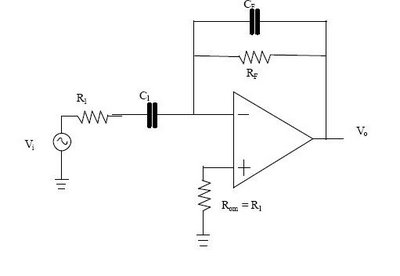
The differentiator circuit is an application circuit derived from mathematical principles influenced by capacitor behavior. The circuit, as illustrated in the accompanying image, is a simple differentiator configuration. To derive the differentiator formula, the following sequence is used: Ic...
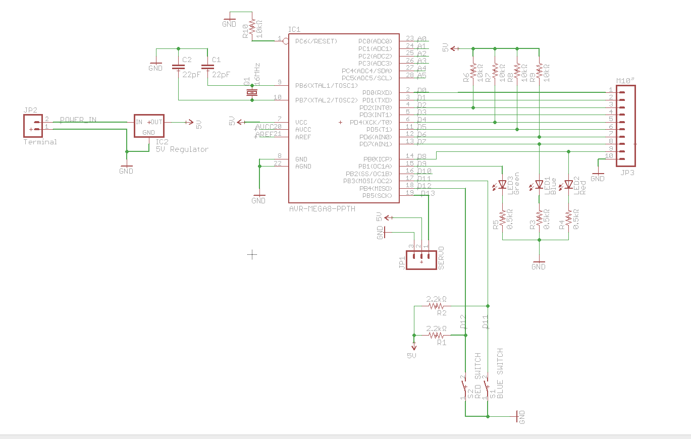
A circuit utilizes a keypad, a servo, and several LEDs, connected to an Arduino Uno. The objective was to integrate all components onto a single PCB, effectively creating a custom version of the Arduino. Upon startup, the red LED...