
Metal detector circuit diagram 6

The metal detector circuit operates by generating an oscillating signal that can be affected by the presence of metallic objects. The probe oscillator generates a frequency signal through the oscillating tube VI, which is influenced by the exploration coil L1. This coil acts as the sensor that detects changes in the electromagnetic field when metal objects are nearby. The capacitors C1 to C4 and resistors R1 to R3 are configured to tune the frequency of the probe oscillator to optimize sensitivity and response time.
The reference oscillator, comprising the oscillating tube V2 and inductor L2, produces a stable reference frequency that is essential for comparison with the probe oscillator's output. The capacitors C6 to C9 and resistors R2 to R4 in this section help in stabilizing the oscillation frequency and minimizing noise.
The oscillation signal processor employs six NOT gates (D1 to D6) to manipulate the signals from both oscillators. The integration of external RC components with these gates allows for further processing of the oscillation signals, enhancing the ability to detect and differentiate metallic signals from background noise.
The mixing amplifier plays a crucial role in combining the outputs from the probe and reference oscillators. The diode YD, along with resistors R12 and R13, and capacitors C13, is configured to rectify and amplify the mixed signals. The field-effect transistor (VF) is used to provide additional amplification, ensuring that the output signal is strong enough to be measured by the ammeter PA.
The choice of transistors V1 and V2 as 59018 silicon NPN types ensures reliable switching and amplification characteristics, while the V20A field-effect transistor is selected for its high input impedance and low output capacitance, which are critical for maintaining signal integrity throughout the circuit.
Overall, this metal detector circuit design effectively combines various electronic components to create a sensitive and reliable detection system for metallic objects, demonstrating the principles of oscillation, signal processing, and amplification in practical applications.The metal detector circuit is composed of the probe oscillator, reference oscillator, oscillation signal processor, mixing amplifier and ammeter PA and other components, and the circuit is shown as the chart. Probe oscillator is composed of the oscillating tube VI, explore coil L1, capacitors C1 ~ C4 and resistors R1 ~ R3 and so on.
Reference osci llator is composed of the oscillating tube V2, inductor L2, capacitors C6 ~ C9 and resistors R2 ~ R4 and so on. Oscillation signal processor consists of six NOT gate (Dl ~ D6) integrated circuit IC and the external RC components.
Hybrid amplifier is composed of the diode YD, resistors R12, R13, capacitors C13 and field-effect transistor VF. V1 and V2 use 59018 silicon NPN transistor. VF selects V20A field effect transistor. 🔗 External reference
Related Circuits

The digital scoreboard circuit is designed to display numerical values ranging from 0 to 9 on a 7-segment display. This display utilizes a common anode configuration. The digital scoreboard circuit operates by controlling a 7-segment display that utilizes a common...
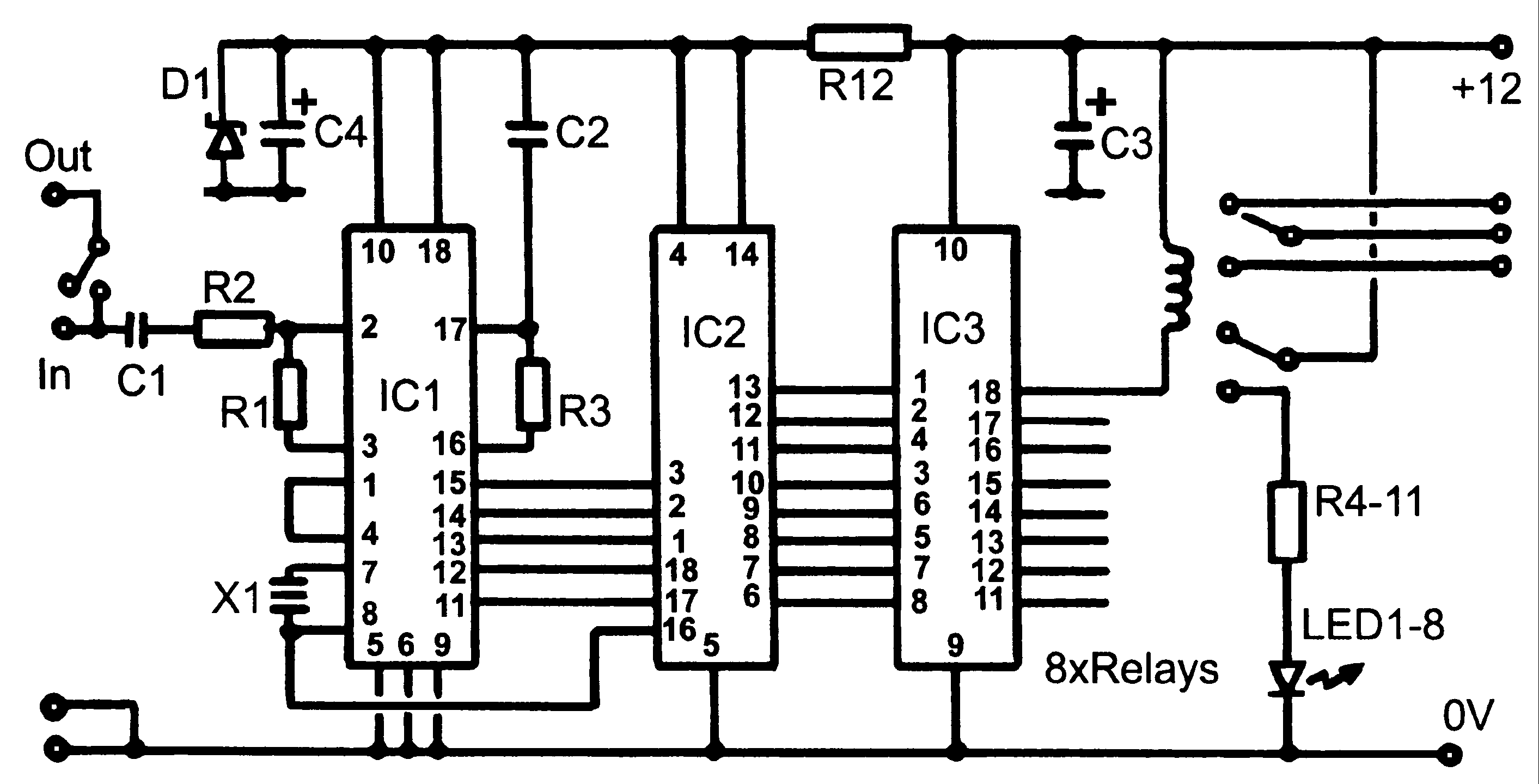
Control monitoring equipment at a TV repeater site is designed to accept commands sent as DTMF tones over the repeater's audio channel. It is capable of switching either AV signals or power supply feeds with currents up to 1...
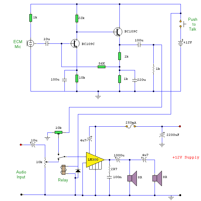
This circuit prioritizes a microphone and preamplifier (voice circuit) over any other audio signal, functioning similarly to a one-way intercom. When the push-to-talk switch is activated, the main amplifier switches from music to the voice signal. Essentially, a voice-over...
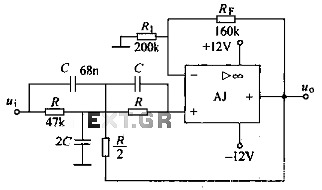
A band-stop filter (BSF) utilizing an integrated operational amplifier is designed to suppress signals within a specific frequency band, allowing signals outside this band to pass with minimal attenuation. This configuration is achieved through a two-stage network, which employs...
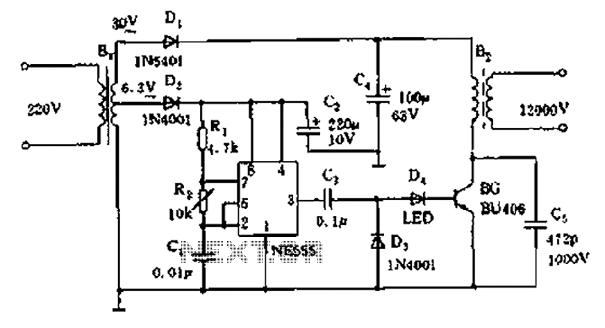
The neon voltage power supply circuit is straightforward to construct, offering stable output power and other desirable characteristics. The core component of this circuit is the NE555 timer, which generates a high-frequency oscillation signal in the range of 15...
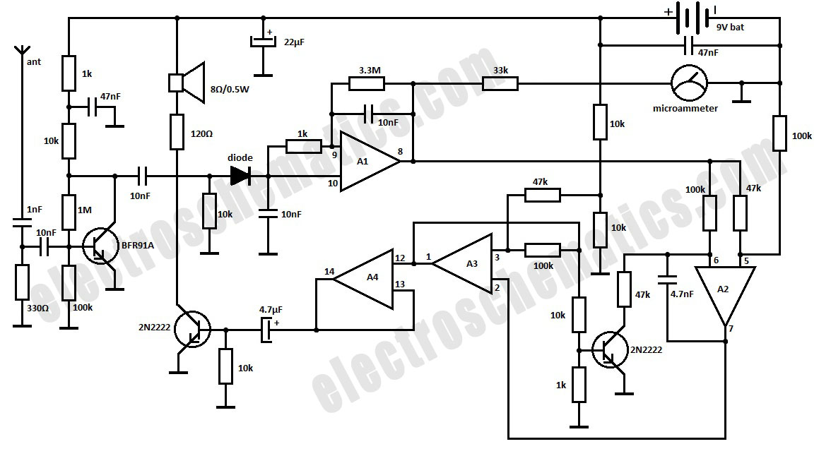
This is a simple RF bug detector designed to identify spy bugs, capable of operating up to 2 GHz. Below are some essential components required for this circuit. The RF bug detector circuit functions by utilizing radio frequency signals...