
Motor vehicle steering flasher 12
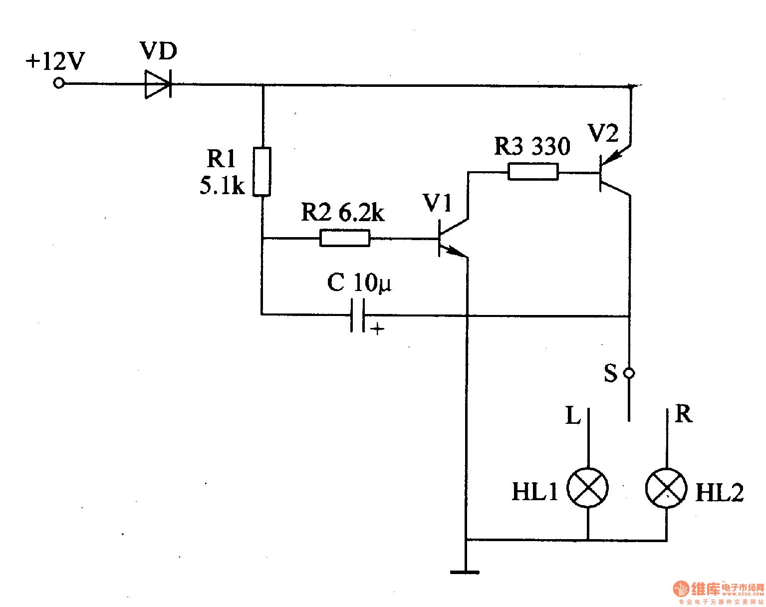
The motor vehicle steering flasher circuit serves as a critical component in automotive signaling systems, enabling drivers to communicate their intent to turn or change lanes effectively. The circuit operates by utilizing a simple oscillator configuration that alternates the current through the turn signal lamps, creating a flashing effect that is easily recognizable to other road users.
The resistors R1-R3 are integral in setting the timing characteristics of the oscillator circuit. The values of these resistors can be adjusted to modify the flash rate of the turn signals, allowing for customization based on vehicle requirements or regulatory standards. The choice of 1/4W carbon film or metal film resistors ensures reliability and stability in performance.
Capacitor C plays a vital role in the timing and stability of the oscillation. The use of a 25V electrolytic capacitor is appropriate for this application, providing sufficient voltage rating to handle the circuit's operational demands while maintaining compact size and efficiency.
The diode VD, specifically the 1N5402, is selected for its robustness and ability to handle higher current loads, ensuring that the circuit remains protected from voltage spikes and reverse polarity conditions. This diode is crucial for rectifying the current and allowing for proper operation of the transistors.
Transistors V1 and V2 are pivotal in controlling the oscillation and signal output. The selection of a silicon NPN transistor (3DGl2 or S8050) for V1 provides reliable switching capabilities, while the germanium PNP transistor (3AD30) for V2 allows for effective modulation of the current flow to the turn signal lamps. The combination of these transistors forms a complementary configuration that enhances the efficiency of the circuit.
Overall, the motor vehicle steering flasher circuit exemplifies a straightforward yet effective design that leverages basic electronic components to achieve reliable vehicle signaling. Proper selection and arrangement of the components ensure that the circuit functions correctly, providing essential safety features for automotive applications.The motor vehicle steering flasher described in the example uses high-power transistors as electronic switches, the circuit is simple, easy to make. The working principle The motor vehicle steering flasher is composed of the flash circuit resistors R1-R3.
Capacitor C, diode VD, transistors V1, V2, it is shown in Figure 7-21. S is the vehicle turn signal switch; HLl and HL2 are the left turn signal and right turn signal respectively. Before turning signal switch S (in the center), the oscillator circuit composed of vl, v2, and external RC components does not work. Placing S in the L or R position, the oscillation circuit works, V2 makes intermittent conduction with a certain frequency, Ll or HL2 is flashing.
Component selection RI-R3 selects 1/4W carbon film resistor or metal film resistors. C uses 25V electrolytic capacitors. VD uses lN5402 silicon rectifier diode. VI selects 3DGl2 or S8050 silicon NPN transistor; V2 uses 3AD30 germanium PNP transistors. 🔗 External reference
Related Circuits

This circuit features an intermittent siren output and automatic reset. It can be operated manually using a key-switch or a hidden switch; but it can also be wired to set itself automatically when you turn-off the ignition. By adding...

Universal motor control with an integrated self-timer. This circuit is designed exclusively for use with motors that have commutators. When expecting heavy motor loads, it is advisable to replace the GE-X1 with a larger-rated C30B SCR for SCR2. To...
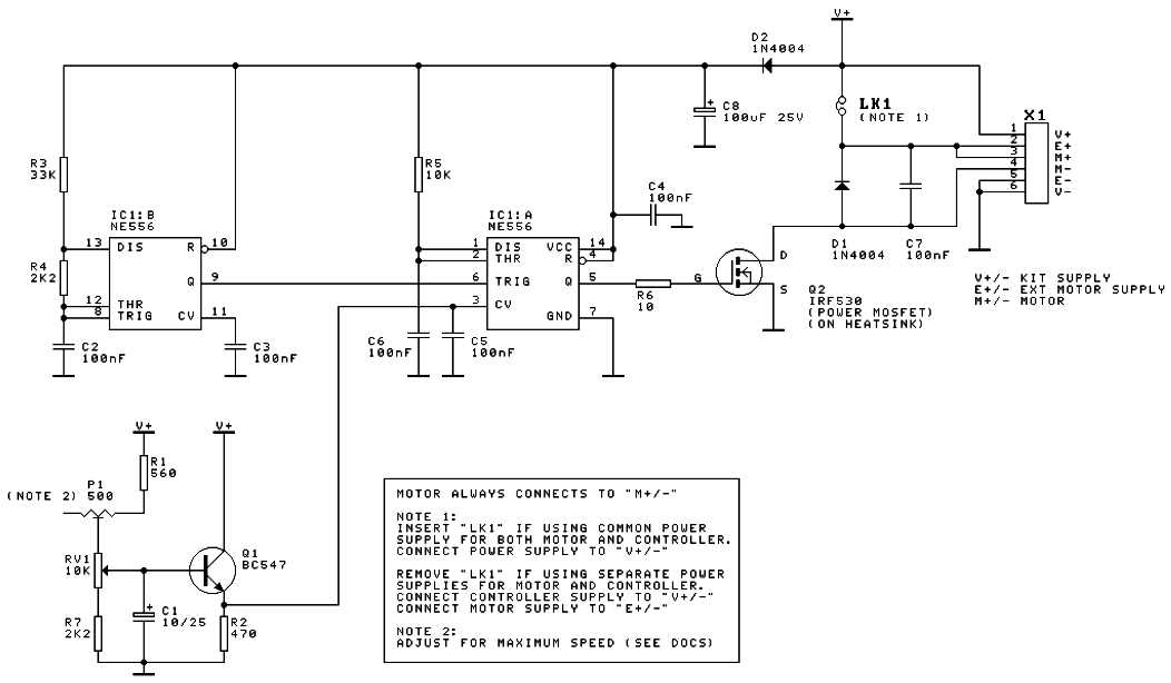
A DC motor speed controller circuit utilizes two timers configured as a Pulse Width Modulator (PWM). The integrated circuit employed for this purpose is the NE556, which is a dual timer/oscillator using NMOS technology. The DC motor speed controller circuit...
Even though the power was off, there was AC present at the handle plug, and a short circuit occurred. Upon disassembly, a blown transistor was discovered. An attempt was made to fix the issue, but after one month and...
The diac is a common component used to trigger triacs. The construction of a diac is similar to that with a transistor, but with both junctions doped to similar levels so that the two junctions' reverse breakdown characteristics are...

A bidirectional H-bridge DC motor control circuit is illustrated. The circuit utilizes the L298 integrated circuit from ST Microelectronics. The L298 is a dual full-bridge driver that supports a wide operating voltage range and can manage load currents up...