
Multivibrator oscillation circuit

The circuit described operates on a resonance principle involving two transistors, VT1 and VT2, and capacitors C1 and Ci. The initial state with VRI off allows the circuit to establish a specific condition where current flows through resistor RJ and capacitor Ci. As VT1 enters conduction, it initiates the charging of capacitor C1. The discharge of C1 produces an inverting charge, which results in a positive voltage across it. This positive voltage subsequently activates VRI.
When VRI is activated, it influences the state of the circuit by closing UC, which in turn applies a negative voltage to the base of VT2. This negative voltage causes VT2 to turn off, interrupting its conduction path. The alternation between the conduction states of VT1 and VT2 creates a feedback loop that sustains the resonance condition. This oscillatory behavior is fundamental in applications such as oscillators or switching power supplies, where controlled timing and energy transfer are essential for efficient operation.
The circuit's performance can be enhanced by selecting appropriate values for the components, such as the capacitance of C1 and Ci and the resistance of RJ, to achieve the desired frequency of oscillation. The design may also incorporate additional components, such as inductors, to further refine the resonance characteristics and improve efficiency. Proper layout and thermal management are crucial to ensure reliable operation, especially in high-frequency applications.It is seen from the ring, when vri off, 0 [2 is turned on, the current through RJ, Ci: When VT1 conduction, charging Cl start discharge. Then give cl inverting charge, I voltage becomes positive, vri turned on. So uc: close O, so that VT2 base electrode becomes negative, VT2 and turned off. Such VT1 and VT2 are alternately turned on and off to form a resonance state,
Related Circuits
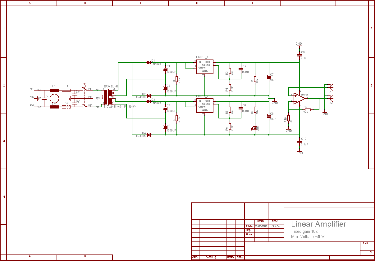
The aim of this project was to develop a linear analogue amplifier designed for laboratory use. This amplifier has to realise a voltage amplification of 10x and is intended to amplify function generator signals for tests. Power supply requirements:...
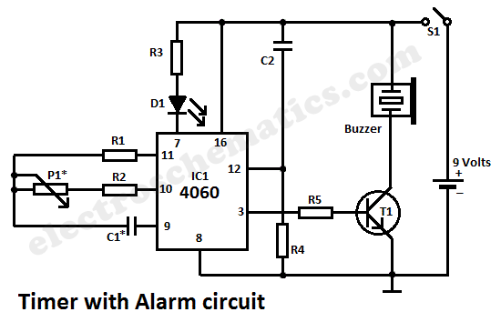
This simple alarm timer circuit is constructed using a 4060 integrated circuit, which features a stable oscillator with a relatively wide frequency range. The alarm timer circuit utilizes the CD4060 IC, which combines a low-frequency oscillator and a binary counter....
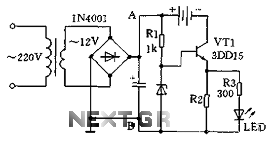
A practical single-tube constant current charger is illustrated, utilizing a transistor (VT1) that plays a crucial role in maintaining a constant current. The current value is determined by the voltage regulator and resistor R2. The general output voltage is...
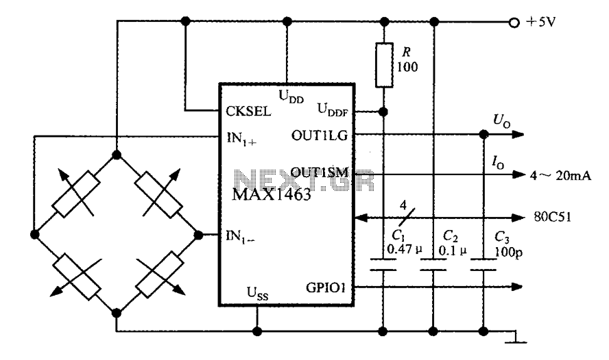
The system consists of a MAX1463 precision pressure detection circuit block diagram. The output voltage from the bridge pressure sensor is connected to the MAX1463 inputs IN1+ and IN1-. Controlled by a CPU, the pressure signal undergoes nonlinear calibration...
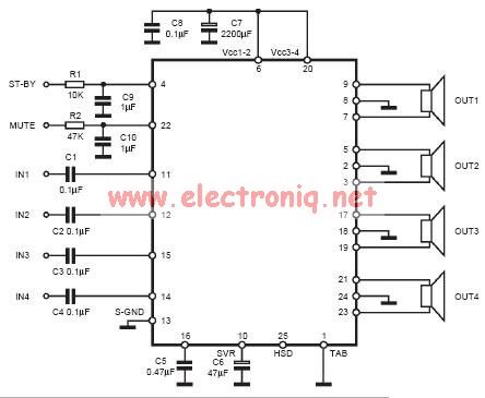
The input capacitor is used for low-frequency cut-off, with a standard value of 0.1 µF, resulting in a cut-off frequency of approximately 16 Hz. The input capacitor plays a crucial role in filtering unwanted low-frequency signals in electronic circuits. By...
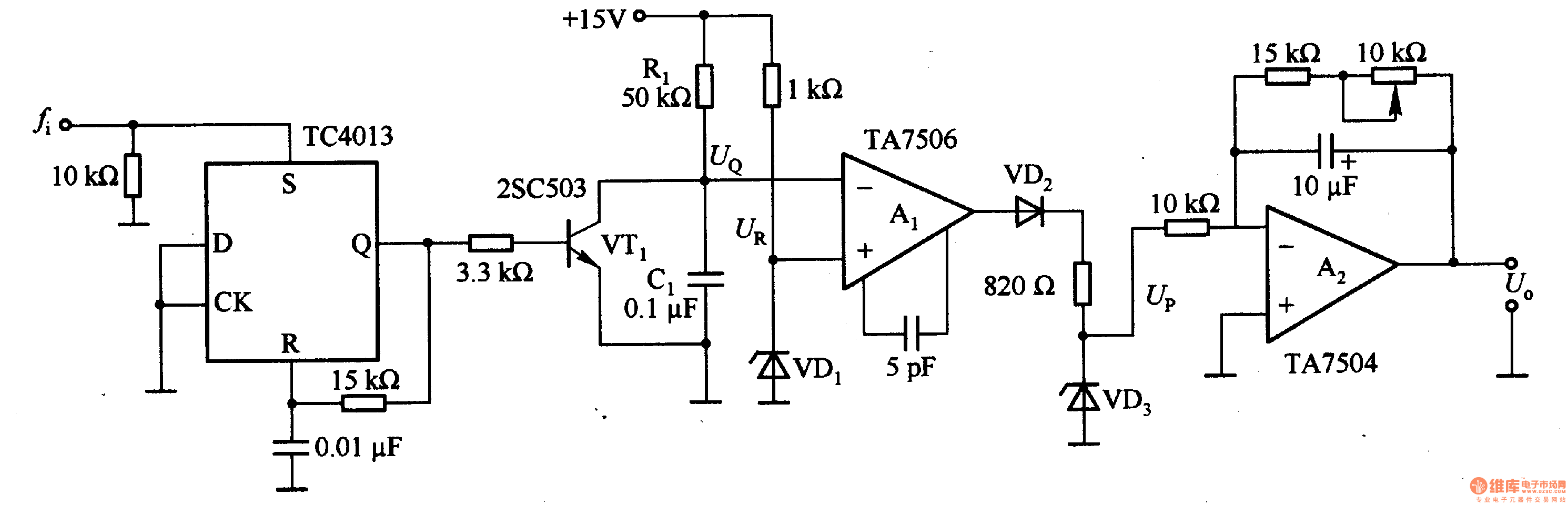
This circuit can convert an input frequency ranging from 0 to 100 Hz into an output voltage of 0 to 10 V. It utilizes the TC4013 monostable multivibrator to shape and amplify the input pulse, which has a width...