
NCP571 low power regulator

The NCP571 and NCV571 voltage regulator circuits are tailored for applications where space is limited and efficiency is paramount. These devices are characterized by their low dropout voltage, which allows them to maintain regulation even when the input voltage is only slightly higher than the output voltage. This is particularly beneficial in battery-operated devices where maximizing battery life is critical.
The internal architecture of the NCP571 and NCV571 includes a voltage reference that ensures stable output voltage across varying load conditions. The error amplifier continuously monitors the output voltage and adjusts the gate of the PMOS power transistor to maintain the desired voltage level. This feedback mechanism is essential for the accurate regulation of the output voltage, especially in scenarios with fluctuating load demands.
In addition to the primary regulation function, the NCP571 and NCV571 devices also incorporate protective features such as current limit and thermal shutdown. The current limit function prevents excessive current draw that could potentially damage the regulator or connected components, while the thermal shutdown feature protects the device from overheating by disabling the output when the junction temperature exceeds a predetermined threshold.
The output voltage can be set using external resistors, allowing for flexibility in design to meet specific application requirements. The low quiescent current of 4.0 µA makes these regulators ideal for applications where power conservation is essential, such as in portable devices that rely on battery power.
Overall, the NCP571 and NCV571 voltage regulators provide a compact and efficient solution for generating low regulated voltages in a variety of electronic applications, making them an excellent choice for engineers seeking reliable performance in space-constrained environments.In some electronic projects you will need an unusual regulated voltage, unusual, because the voltage required is very small and you can not use zenner diodes or some other tricks due of a compact design. In that case you can use this voltage regulator circuit based on the NCP571, NCV571 which are low current voltage regulators available in few
standard output voltage versions ( 0. 8 V, 0. 9 V, 1. 0 V and 1. 2 V ). The NCP571, NCV571 low dropout linear regulators are designed for handheld communication equipment and portable battery powered applications which require low quiescent current. The NCP571, NCV571 series features an ultra ’low quiescent current of 4. 0 uA. NCP571, NCV571 device contains a voltage reference unit, an error amplifier, a PMOS power transistor, resistors for setting output voltage, current limit, and temperature limit protection circuits.
🔗 External reference
Related Circuits
Power line fluctuations and cut-offs can damage electrical appliances connected to the line, particularly domestic appliances like refrigerators and air conditioners. When a refrigerator operates on low voltage, excessive current flows through the motor, leading to overheating and potential...
New cellular phones have incorporated high-resolution cameras that require bright illumination of the surrounding area to achieve high-quality pictures. Traditional xenon-filled photo flashes cannot be used due to the limited space available in cellular phone cameras. Instead, design engineers...
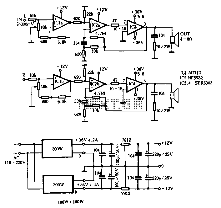
The T amplifier circuit schematic section is illustrated in Figure 3-51. It utilizes the Japan Sanyo STK6303 Pina, which is a high-power thick film integrated circuit. The maximum power supply voltage is 36V, and the output current can reach...
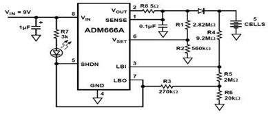
The ADM666A application note provides a detailed explanation of a low-cost battery charger circuit, including maximum output voltage, charge termination voltage calculation, battery voltage level monitoring, and circuit efficiency optimization. The ADM666A utilizes an NPN transistor and a P-channel...
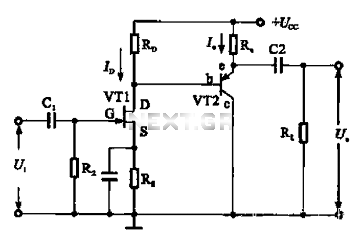
The circuit consists of a grounded source and an emitter follower configuration. The source is grounded, and the emitter is combined with a common-collector transistor amplifier. As shown in the figure, VTI is a vibration-grounded field-effect transistor amplifier, while...
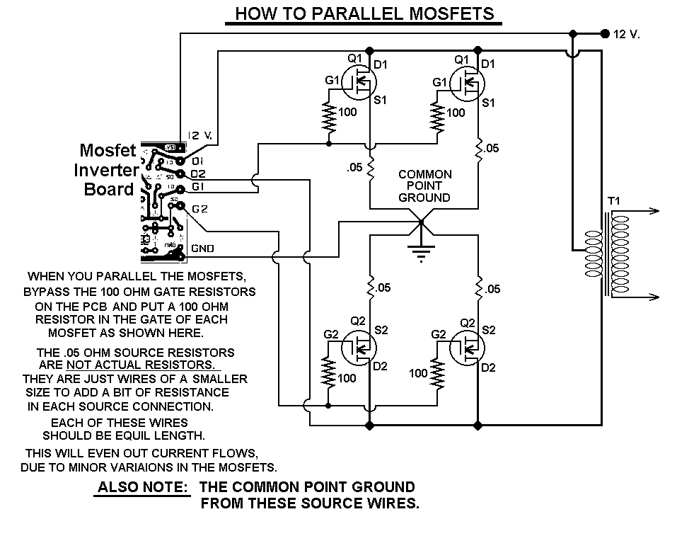
This 1000-watt power inverter circuit diagram is based on the MOSFET RF50N06. For increased power output, additional MOSFETs can be paralleled with the RF50N06. These MOSFETs are rated for 60 volts and 50 amps. It is essential to connect...
Warning: include(partials/cookie-banner.php): Failed to open stream: Permission denied in /var/www/html/nextgr/view-circuit.php on line 713
Warning: include(): Failed opening 'partials/cookie-banner.php' for inclusion (include_path='.:/usr/share/php') in /var/www/html/nextgr/view-circuit.php on line 713