
One-touch turn signal module N version
.png)
The OTTS module is designed to provide enhanced functionality to traditional turn signal systems in vehicles. The integration of a microcontroller, specifically the Atmel ATtiny24, allows for programmable logic that can adapt to various user preferences and vehicle configurations. The use of a low-dropout voltage regulator (LM2931Z-5) ensures that the microcontroller operates reliably within the automotive environment, which can often present voltage fluctuations due to the vehicle's electrical system.
The design includes a four-way DIP switch that allows users to select different operational modes, catering to individual preferences for signal duration and cancellation. The inputs from the turn signal lever are directly interfaced with the microcontroller, enabling the OTTS module to process user commands effectively.
The output stage employs N-channel MOSFETs (T5 and T6) for switching the turn signal lamps. The choice of TO-220 package for these MOSFETs facilitates efficient heat dissipation, crucial for maintaining performance under high load conditions. The circuit is designed to handle significant current loads while minimizing heat generation, which is essential for long-term reliability.
To enhance the robustness of the design, additional protective components such as Zener diodes and standard diodes are included to safeguard against voltage spikes and reverse currents, ensuring the longevity of the MOSFETs and overall circuit integrity. The optional LEDs provide diagnostic feedback, allowing for easier troubleshooting during installation or maintenance. This comprehensive design approach ensures that the OTTS module not only improves user experience but also adheres to automotive standards for safety and reliability.The one-touch turn signal (OTTS) module enhances the functionality of the turn signal lever by adding a mode where a single touch makes the indicators blink for a certain number of times. This behavior is also known as lane change turn signal or comfort blinker. This sub-article describes one of the variants of the OTTS module, the N version. This variant is for electrical systems where the turn signal lever switch drives the turn signal lamps directly and a single-pole flasher relay switches between the shared contact of the turn signal lever switch and the negative terminal. For more information about the OTTS module or other variants refer to the one-touch turn signal module main article.
As is the case with many microcontroller based projects the circuit diagram is rather simple. Since all logic is inside the controller`s program memory, the diagram does not reveal much of the working. The heart of the diagram is IC1 the microcontroller. The OTTS module is built around an Atmel ATtiny24, an inexpensive yet versatile microcontroller. IC2 is a LM2931Z-5 low-dropout voltage regulator and supplies the Atmel microcontroller with a stabilized 5 V.
This isolates the sensitive controller from the hostile power environment of the car and ensures stable operation. The rest of the circuit is less critical and operates directly at the 12 V battery voltage. Left from the controller are the inputs. Four-way DIP switch S1 is used to select the presets for the comfort mode and the canceling. Inputs IN_LEFT and IN_RIGHT are connected to the turn signal lever switch. On the right side of the controller are both output stages the bottom half is the same as the upper half but drawn mirrored.
Switching is performed by N-channel MOSFETs T5 and T6. MOSFETs are reliable and inexpensive solid state devices that can switch large currents. The OTTS module requires N-channel MOSFETs in a TO-220 package with a maximum gate-source voltage VGS of over 15 V. The MOSFET internal resistance RDSon plays an important factor in the choice of MOSFET. The higher RDSon the more heat is dissipated in the MOSFET for a given current. The TO-220 package can dissipate up to 2 W without heat sink, but it is recommended to stay below 1 W when the module is mounted in a small closed box.
For example for a current of 5 A the maximum RDSon at 1 W can be calculated as follows: Thus to switch the 5 A load, MOSFETs with RDSon of 0. 04 © or lower must be chosen for example the Fairchild Semiconductor HUF75339P3 N-channel MOSFET with RDSon of 0.
012 ©. The efficiency of most MOSFETs is best when the gate-source voltage VGS is 10 V or more but the Atmel microcontroller operates at only 5 V. Therefore each MOSFET is driven by a double common emitter circuit around transistors T1 to T4. When the output stage gets a high signal from the microcontroller, current flows through the base of the first transistor, driving it into saturation and making it conduct.
This pulls the base of the second transistor to the ground the second transistor does not conduct. The MOSFET gate is at the same level as the 12 V battery voltage. Since the MOSFET source is connected to the ground, the voltage over gate and source (VGS) is now 12 V. The MOSFET conducts and current can flow through the load. When the microcontroller outputs a low signal, the double common emitter circuit pulls the MOSFET gate to the ground.
VGS is then 0 V and the MOSFET does not conduct. LEDs D1 and D2, and their current-limiting resistors R11 and R12 are optional. The LEDs provide visual feedback of the outputs which may come in handy when diagnosing but are otherwise not needed. Zener diodes D3 and D4 protect the MOSFETs` gate (input) against overvoltages and diodes D5 and D6 protect the MOSFETs against reverse polarity kickback voltages from inductive loads like relays.
When the module has to drive large relays with nominal coil currents over 150 mA, it is rec 🔗 External reference
Related Circuits
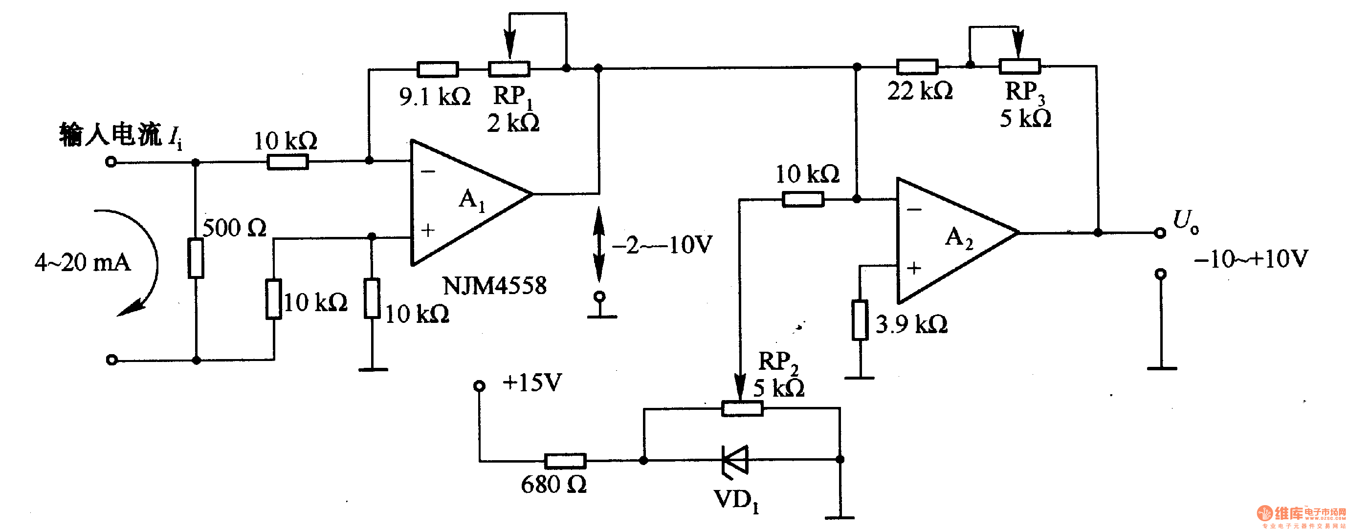
Figure 1-42 (a) is a voltage/current conversion circuit that converts a 0-10V input voltage into a 4-20mA output current. Adjusting resistor RP2 can set the input voltage (Ui) to 0V, resulting in an output current (I) of 20mA; similarly,...
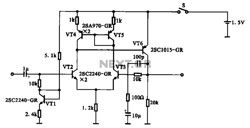
A 1.5V-powered microphone signal amplifying circuit is designed with a power supply for the microphone signal amplification. The circuit primarily consists of a differential amplifier formed by transistors VT2 and VT3. Additionally, VT6 functions as a common emitter voltage...
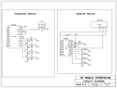
This document presents a circuit example for interfacing an RF module using the HT12E/D encoder-decoder pair. The attached circuit can be utilized for data transmission via the RF module, which is designed for single-channel operation, allowing only serial data...
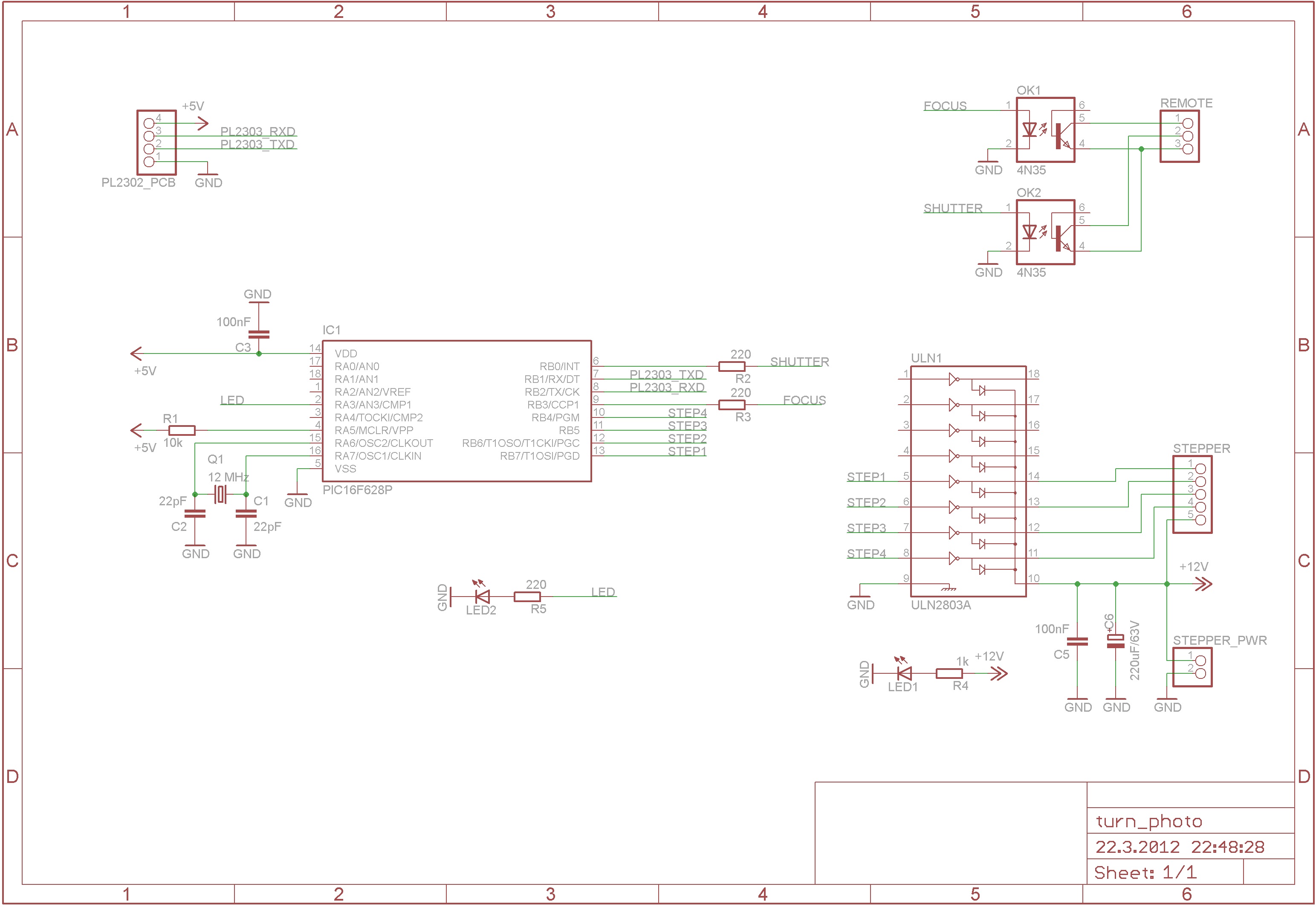
The device captures 360-degree photos, which are essentially animations made from multiple images of a product taken from different angles. It requires a controllable device that can take pictures at even intervals. As depicted in the accompanying image, a...
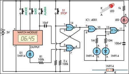
This device serves as a daily medication reminder. It incorporates a crystal watch and a 4001 quad 2-input NOR gate, with two of the gates (IC1a & IC1b) configured as an RS flip-flop. The watch is programmed to alert...
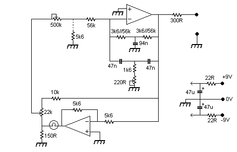
The output level was set to 3.8V peak to peak. The initial objective was to compare several different operational amplifiers (op-amps) before further optimizing the circuit. The op-amps evaluated were the TL072, LM4562, and OPA2134. The distortion spectra are...