
Open-Loop Peak Detector Circuit
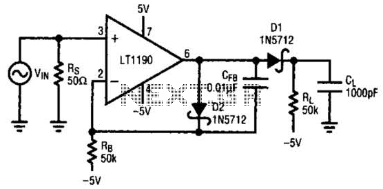
In this open-loop configuration, the circuit utilizes two diodes, D1 and D2, to facilitate signal detection and compensation. D1 serves as the primary detector diode, while D2 functions as a compensating diode, ensuring that both diodes experience equal voltage drops due to the use of matched resistors. The load resistor RL, connected to a -5 V supply, plays a critical role in determining the circuit's response speed. The identical bias resistor RB, also connected to -5 V, is essential for establishing the operating point of the compensating diode.
The choice of resistor values is pivotal in balancing the circuit's performance characteristics. Low resistance values for RL and RB, typically ranging from 1 kΩ to 10 kΩ, enable rapid response times, making the circuit suitable for applications requiring quick signal processing. However, this speed comes at the cost of reduced accuracy at low frequencies, as the circuit may not adequately respond to slower signal variations.
Conversely, selecting higher resistance values for RL and RB enhances low-frequency accuracy, allowing the circuit to better track slow signal changes. Nevertheless, this configuration can lead to limitations in high-frequency performance due to the amplifier reaching its slew rate limit. This phenomenon occurs when the amplifier cannot respond quickly enough to rapid changes in the input signal, resulting in distortion or loss of fidelity in high-frequency applications.
To optimize the circuit's performance across a range of frequencies, the inclusion of a feedback capacitor CFB is recommended. This capacitor enhances the negative slew rate of the amplifier's negative input, allowing for improved handling of rapid signal transitions while mitigating the adverse effects of high-frequency limitations. The careful selection of component values and the strategic addition of feedback elements are essential in achieving a well-balanced circuit capable of performing effectively in diverse electronic applications. In this open-loop design, the detector diode is Dl, and a level shifting or compensating diode is D2. Load resistor RL is connected to -5 V, and an identical bias resistor RL is connected to -5 V, and identical bias resistor RB is used to bias the compensating diode.
Resistors with equal values ensure that the diode drops are equal. Low values of RL and RB (1 kU to 10 kf2) provide fast response, but at the expense of poor low-frequency accuracy. High values of RL and Rn provide good low-frequency accuracy, but cause the amplifier to slew rate limit, resulting in poor high-frequency accuracy.
A good compromise can be made by adding a feedback capacitor CFB, which enhances the negative slew rate on the (-) input. 🔗 External reference
Related Circuits
This circuit consists of two main components: a battery charger that provides a fixed output voltage of 5V DC, and a regulated power supply that allows for an adjustable output voltage ranging from 2 to 9 volts. The circuit design...
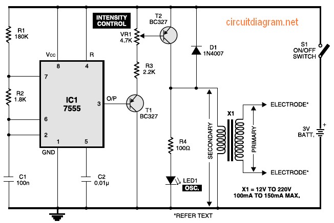
Figure 1 shows the circuit of a muscular stimulator. The IC 7555 is configured as an astable multivibrator to generate approximately 80Hz pulses. The output from IC1 is connected to transistor T1, whose emitter is linked to the base...
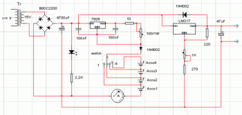
This blog provides insights into SMPS (Switched-Mode Power Supply) circuit diagrams. It offers valuable information for those interested in understanding this topic. Switched-Mode Power Supplies (SMPS) are crucial in modern electronic devices due to their efficiency and compact design. An...
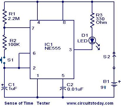
When switch S2 is activated, the circuit functions as an astable multivibrator, causing the LED to illuminate for approximately 0.1 seconds, flashing every 1.5 seconds. Due to the human reaction time being greater than this duration, it is unlikely...
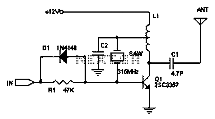
The circuit principle involves the use of an LC oscillator, which typically experiences significant frequency drift. Surface Acoustic Wave (SAW) devices have emerged as a solution to this issue, offering frequency stability comparable to that of crystal oscillators. SAW...
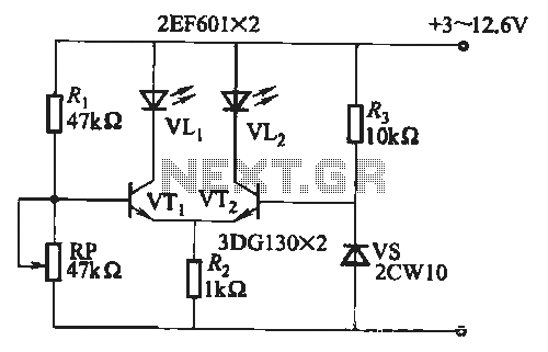
When the battery voltage is within the range of 7 to 12.6V, the light-emitting diode VLi illuminates, maintaining a consistent brightness. If the battery voltage drops below 7V, VLi begins to emit a red light, and the brightness of...