
CCD analog output signal processing circuit diagrams
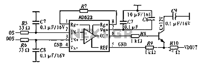
The AD623 amplifier is designed for applications requiring precise signal amplification with minimal interference from common-mode signals. Its high CMRR ensures that differential signals can be accurately amplified while rejecting noise and interference that may be present in the common mode. The low voltage drift characteristic is critical for applications where stable performance over varying temperatures is essential.
The programmable gain control feature allows users to set the gain of the amplifier according to the specific requirements of the application, which can be achieved by connecting an external resistor to the appropriate pins. This flexibility makes the AD623 suitable for a wide range of applications, particularly in sensor signal processing where the input signal levels may vary significantly.
In the context of CCD analog signal processing, the AD623 plays a crucial role in maintaining signal integrity. The amplifier's design facilitates the handling of video signals, which are often subject to fluctuations and noise. By compensating for the inverting and non-inverting inputs, the amplifier ensures that the output signal remains stable and reliable.
The output stage of the AD623 is configured as an emitter follower, which enhances the amplifier's ability to drive loads effectively. This configuration provides a high input impedance and low output impedance, allowing for efficient signal transfer to subsequent stages in the circuit without significant signal degradation.
Overall, the AD623 is an effective solution for applications demanding high precision and stability in signal amplification, particularly in environments where temperature variations and common-mode noise are concerns. Its integrated design simplifies circuit implementation while improving overall performance.AD623 integrated 3-way amplifier. Single or dual supply can work with high CMRR and low voltage drift, programmable gain control in addition to an external resistor, all compon ents are integrated in the interior temperature of the circuit to improve the stability and reliability. Application of AD623 in CCD analog signal processing circuit shown. The video signal output, respectively, and compensation to the AD623 inverting and non-inverting input.
In AD623 output stage emitter follower termination to enhance the driving capability of the signal. The selection device can eliminate the use of ordinary temperature op amp and peripheral resistance caused by the output signal drift.
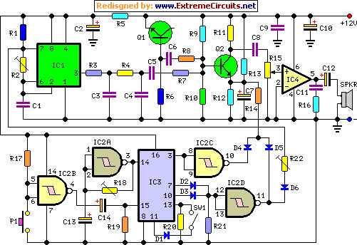
Related Circuits
Both circuits can synchronize trapezoidal wave voltage, which is converted into intermittent small rectangular pulses. Its working principle involves periodic operation in synchronization with the grid frequency of the zero-volt switching voltage of the DC chopper. Due to the...
The multivibrator flashing light emitting diode (LED) display driver circuit can be utilized in toys, creating flashing effects in the eyes of animals or monsters. This circuit employs a multivibrator configuration, typically a 555 timer IC or a similar component,...
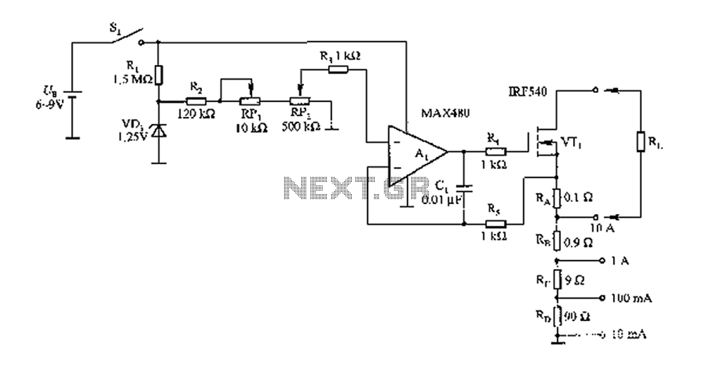
The FIG load test is a control circuit designed for external loads up to 10A, commonly utilized in drive test power applications, power amplifiers, LED solenoids, and relays. It is capable of handling various resistive loads and features a...
This circuit generates a two-tone effect similar to the cuckoo song. It can be used for doorbells or other applications due to a built-in audio amplifier and loudspeaker. As a sound effect generator, it can be connected to external...
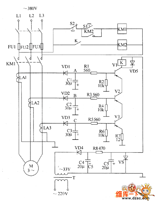
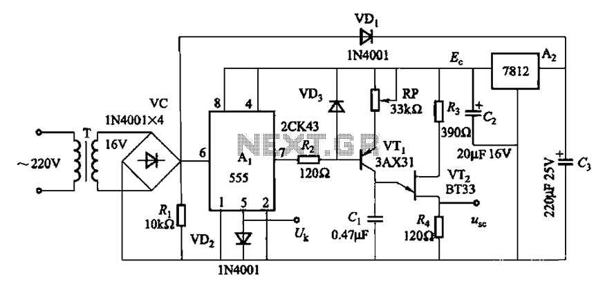
The motor protection circuit consists of a power supply circuit, a current detection circuit, and a protection control circuit, as depicted in the accompanying diagram. The power circuit includes a power transformer (T), a rectifier diode (VD4), filter capacitors...
The installation involves a solid-state OEM water depth sensor designed for continuous fluid level measurement. This sensor outputs a resistive signal that is inversely proportional to the liquid level: as the liquid level decreases, the output resistance increases, and...