
Switch control circuit diagram mcu

The circuit operates with a focus on efficiency and safety, ensuring that the power supply can be activated and deactivated seamlessly through the microcontroller's control logic. The design incorporates feedback mechanisms via the optocouplers, which facilitate communication between the power supply circuit and the MCU, enabling precise control over the power state. The use of a push-button switch (SB) simplifies user interaction, while the soft start feature prevents sudden power surges that could damage connected peripherals. The inclusion of EEPROM storage for state retention during power loss enhances the reliability of the system, making it suitable for applications where data integrity is crucial. The overall architecture reflects a well-thought-out approach to managing power supply operations in electronic devices, particularly those requiring stable and controlled power input, such as printers and other computing peripherals. As shown in FIG TOPSwitch FZ chip switching power supply circuit diagram is controlled by the MCUs. The microcontroller can use inkjet printers, laser printers and other comput er peripherals TOPSwitch FX constituted by a switching power supply control circuit shown in Fig. Switching power supply mainly composed TOPSwitch FX (IC1), optocoupler (IC2) components. The control circuit includes a microcontroller (MCU), two LTV817A linear optocoupler (IC3, IC4), push button switch SB. Signal is generated only when you press the SB is only valid when lifting signal does not work. The SB would not need anti-shake circuit, because the switching power supply soft start time (about 10ms) and the MCU initialization and reset delay time can play a role, you can avoid the time jitter interference when pressed SB; and only when the switch is pressed at least to achieve the above time, the switch to turn on the power by MCU.
This will require the SB press in the end, instead of single click, to ensure power supply starter. After the completion of MCU initialization and reset detected IC3 sent to the start signal, and then go through the power lock switch IC4. Optocoupler IC3, IC4 of LED light tube and phototransistor, respectively LED3 and VT3, LED4 and VT4 representation.
Now LED3 connected between the control terminal and the SB upper, VT3 connected to the logic input MCU. No current through LED3 under normal, IC3 does not work. Logic output MCU through isolation diodes and resistors R4 VD6 then positive LED4 of. VT4 is connected between the M, S end. M by itself end limiting function, it does not require additional VT4 limiting resistor. CM multifunctional end noise cancellation capacitor. When a user first press SB, VD4 conduction, M and S pole end through VD4 turned, TOPSwitch FX namely in three terminal mode, multi-function terminal (M) and switching frequency setting terminal (F) does not work, the current through LED3 on this point, VT3 give MCU start signal.
If the power switch is initially in the OFF state (M-side floating) for the first time the power is turned on by pressing SB, + 5V output voltage UCC provides operating power supply voltage for the MCU. MCU orders after receiving a start signal VT4 conduction, switching power remains in the ON state, the normal output.
When the user presses again on the issue of SB shutdown signal, MCU receives the signal after the implementation of the shutdown procedure, the ink jet printer head stop at a safe place. Once you perform the shutdown procedure, MCU will make it VT4 off the M terminal vacant, switching power shutdown mode, when TOPSwitch FX in a low power state, when UI 230VAC the chip consumes only 160mW.
If the DVD is used when the power switch, the shutdown procedure and the data set state can be stored in the E2PROM, yet they are not lost even after power failure.
Related Circuits
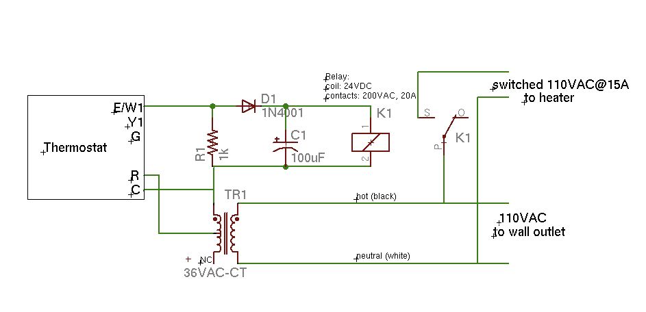
A basic schematic of the circuit is presented, marking the initial experience with Eagle software. It is important to note that only the W1 output of the thermostat is utilized, while C serves as the common connection. The schematic outlines...

A circuit designed to operate within a frequency range with an accuracy greater than 2% for generating Bode plots. It converts two sine waves into a square wave, taking into account the overlap relative to the total input wave...

This circuit allows multiple cameras to be connected to a single monitor. It can be operated either manually or automatically. In automatic mode, a switch is connected to the output of a 555 astable multivibrator, which generates a continuous...

A light dimmer circuit is used to adjust the illumination of a lamp. The following circuit illustrates a basic TRIAC triggering circuit that utilizes a DIAC. In this circuit, the illumination of the light is regulated through the interaction...

This circuit demonstrates a typical six-digit dynamic display configuration. It utilizes the PA 8255 for display output code and the PB port for bit selection code. The display buffer is designated as DISBUF, which processes the hexadecimal number obtained...

This circuit produces a soft turn-on for halogen lamp filaments upon powering up. The MOSFET used is a BUZ10, which has a resistance of 0.2 ohms. Resistors R1, R2, and capacitor C1 set the turn-on rate, while diode D1...