
PC ROM emulator circuit
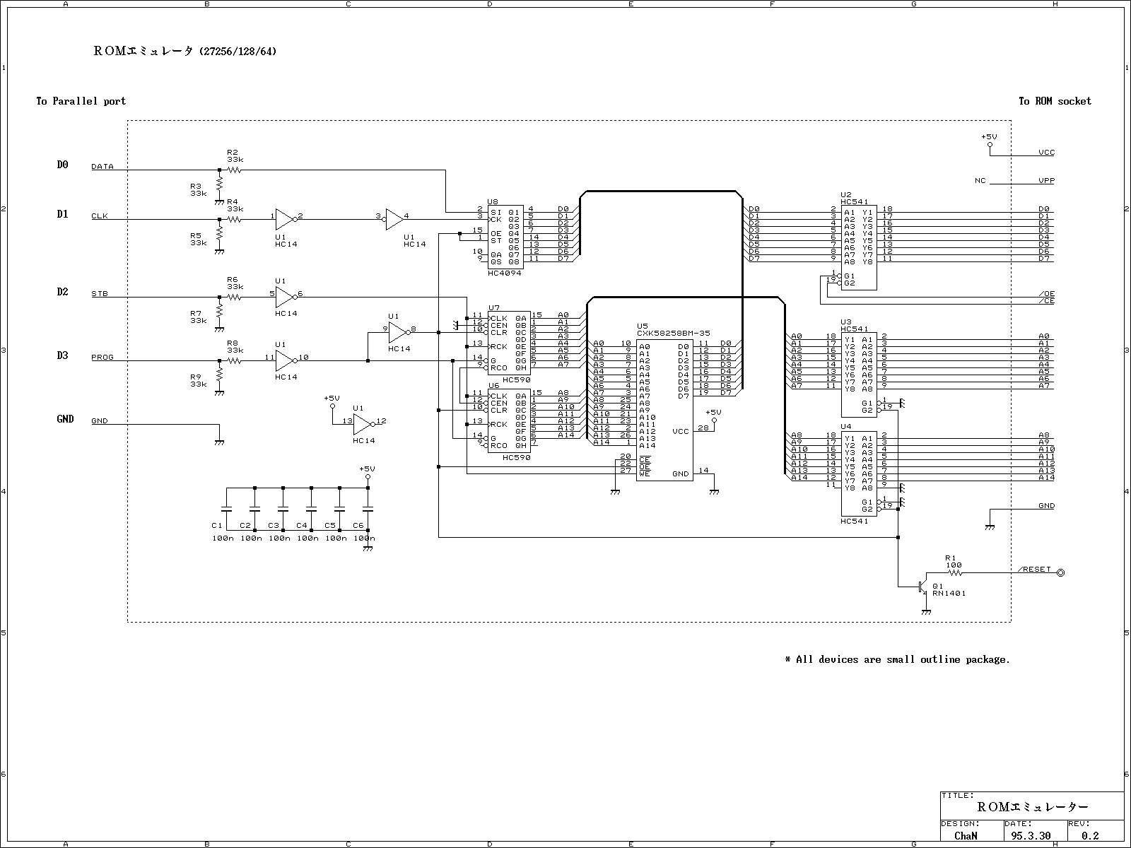
The ROM emulator circuit is designed to replicate the behavior of specific ROM types (2764, 27128, and 27256) while minimizing the physical footprint of the device. The circuit utilizes surface mount technology (SMT) components to achieve a compact size, with a target dimension of 69 mm x 47 mm x 5 mm. The board layout prioritizes efficient routing of power and signal lines to ensure reliable operation, with power lines wired using TA (0.5 mm diameter) and signal lines using UEW (0.2 mm diameter).
The emulator operates in two primary modes: Running Mode and Data Transfer Mode. In Running Mode, the PROG signal is set to low, allowing the target system's address to be routed to the buffer RAM (U3 and U4), enabling data retrieval. The output from the address counters (U6 and U7) is disabled to prevent unintended access to memory during this phase.
Upon transitioning to Data Transfer Mode by setting the PROG signal high, the emulator disconnects the address input from the buffer RAM and enables the address counter, facilitating the writing of data to the RAM. The data is shifted into the shift register (U8) with each clock pulse, and upon receiving a positive pulse on the STB line, the data is written into the buffer RAM sequentially.
To ensure proper operation, a RESET probe should be connected to the target system during data transfer to avoid erroneous reads. The design accommodates both SOP and DIP ICs, with a recommendation for DIP due to availability constraints. The emulator's architecture is straightforward, relying on standard logic components, which simplifies sourcing and assembly.
Overall, this ROM emulator provides a practical solution for developers needing to emulate legacy ROM types while maintaining a compact form factor and straightforward operational capabilities.This ROM emulator improves the easiness to build/use it by reducing down its function which can be used as a ROM emurator. The kind of the ROM types to be emulated, are 2764, 27128 and 27256. The debugging capability is only Load and Run, omit functions such as trace or step execution. It will still sufficient because Load and Run is used mainly even if using an ICE. No power requiment. Operating power is supplied from the target system. However, the data on the buffer memoly is not held when the target power is down. Therefore, the data must be sent again after power is up. Use a PC to control the ROM emurator via a parallel port instead of an interface board to attach it to the various PCs easily.
Build the ROM emulator as small as possible. Let's try a limit of the miniaturization this time, the card size is a goal. Because a goal is card size, all the parts to be used are surface mount devices. All parts are mounted on the settlement side of the proto-board of 50mils pitch. First, after the position of the ICs is decided, wire in the order of the power line and the signal line. It is good when TA(0.5mm dia) is used for the power lines and UEW(0.2mm dia) is used for the signal lines.
Wire signal lines as route between the IC's. The wire is connected with pre-soldering because it cannot be wound to the lead of the ICs. Be careful because it becomes the end and has difficulty if it isn't wired with thinking about the wire density. When wiring is finished and operation is confirmed, cover the circuit board with thin plastic board. The part inside dashedline of the circuit diagram could be built within the size of 69mm x 47mm x 5mm as a result of the try to the miniaturization.
The goal was decided to be attained with ease because it was card size. The power lines that signal returns, of the connection cable from the ROM emurator to ROM plug, are only two. You had better shorten it as much as possible. There was no special part in the junk box, I used only standard logics. When you couldn't obtain SOP ICs, DIP ICs can be used. I recomment to use DIP ICs instead of SOP ICs. When PROG signal goes "Low", the ROM emulator enters Running Mode. The address from the target system is inputted to buffer RAM via U3 and U4. The read data from the buffer RAM can be read from the target system via a data buffer (U2). The value of address counters (U6, U7) is cleared to zero, and its output is disabled. The data shift register also be disabled. Data transfer mode: When the PROG goes "High", the ROM emulator enters the data transfer mode. The address input from target system is disconnected from the buffer RAM, and the counter output is enabled and input to RAM as the address to be transfered.
The reset of the counter is disabled, and the counter gets able to count-up. Output of the buffer RAM is disabled, and the output of shift register (U8) is enabled and input to the buffer RAM. In data transfer mode, to prevent faulty operation of the terget system, the RESET probe should be connected to reset generator on the terget board.
Because the read data from target system becomes wrong. To write data into buffer RAM: DATA is shifted in into the shift register with rise edge of the CLK. Send data to the shift register in order from MSB. When positive pulse is given to the STB, data in the shift register is written into buffer RAM, and the address counter is incremented. The first STB is invalid, and an address 0000h is output after that. (due to specifications of 74HC590). An STB pulse must be applied after enter data transfer mode before start to transfer. Write all data from the first address by repeating 3 and 4. When emurate 2764 or 27128, whole buffer RAM(32KB) including images must be filled, because A13 and A14 may be left unconnected.
Make PROG "Low" after the data transfer is finished, the reset is released, the target system will start. 🔗 External reference
Related Circuits
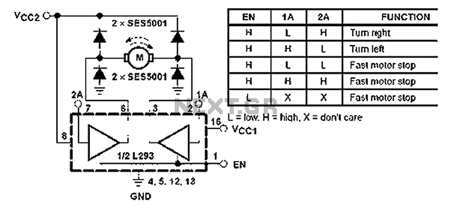
All inputs are compatible with TTL. Each output consists of a complete totem pole driver circuit, utilizing Darlington transistors and pseudo-Darlington sources. The driver enable signals, labeled as 1,2 EN and 3,4 EN, control the activation of drivers 1...
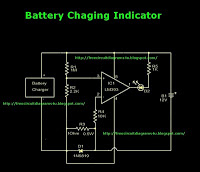
This is a battery charger indicator circuit diagram. When the battery is charging, it is indicated by an LED. This circuit can be used with a 12V battery with a charging current of less than 1A. The battery charger indicator...
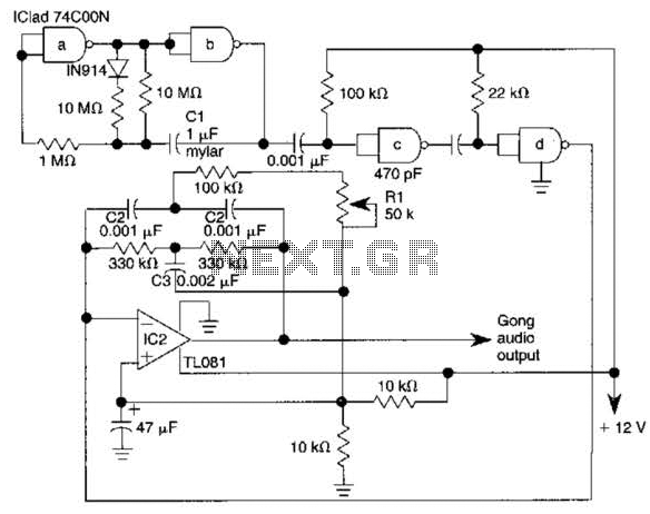
The electronic gong consists of an oscillator utilizing half of a 74C00 quad 2-input NAND gate, an active twin-T filter based on a TL081 operational amplifier, and an audio amplifier integrated circuit, such as the LM386N. Pulses generated by...

The circuit is designed to regulate a dual power supply that provides +12V and -12V from the AC mains. Such a power supply is an essential tool for an electronic hobbyist's workbench. The schematic of the circuit includes components...
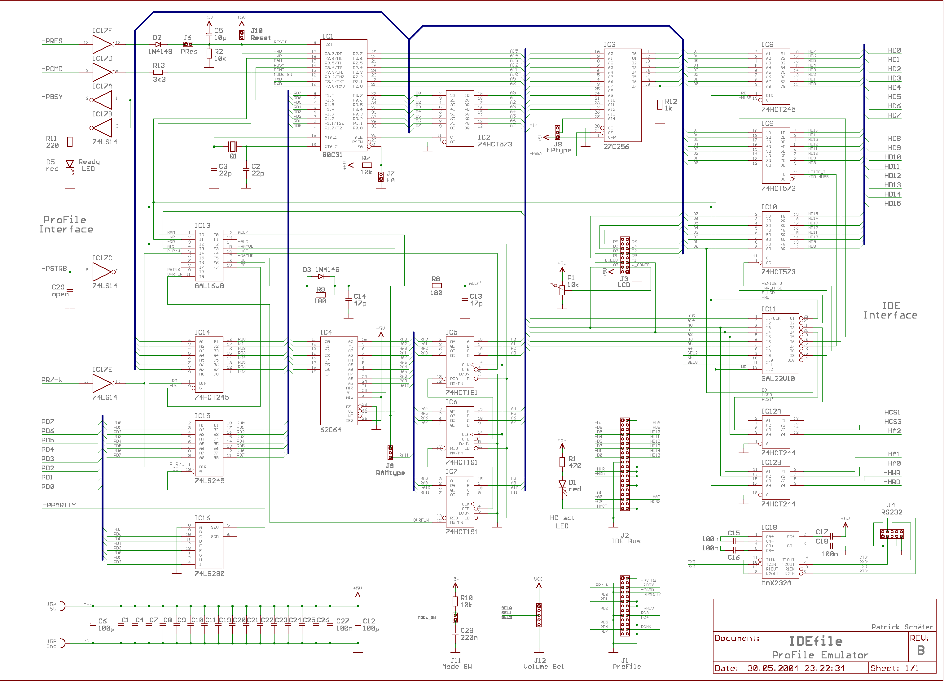
This interface has become a standard for nearly all operating systems known today. IDEfile is a ProFile-compatible hard drive designed for Apple /// and Lisa systems. It emulates the classic 5MB ProFile and the rare ProFile 10M. There are...
In a lithium-ion cell, a voltage of 3.8V per cell indicates a state of charge of approximately 50%. It is important to note that using voltage as a fuel gauge is not precise, as cells manufactured by different companies...