
Phase Shifter
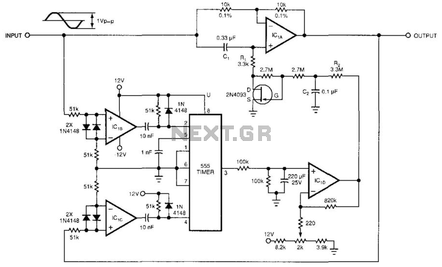
The circuit operates by leveraging the characteristics of a JFET to achieve variable resistance, which is crucial for adjusting the phase shift. The use of the 555 timer as a phase detector allows for precise measurement and control of the phase relationship between the input and output signals. The zero-crossing detectors (IC1B and IC1C) ensure that the phase detection is accurate by responding to the zero crossings of the input and output waveforms, effectively providing a clean transition for the 555 timer to process.
The diodes D1 and D2 serve to protect the 555 timer inputs from excessive voltage levels, ensuring that the circuit operates within safe limits while maintaining signal integrity. The filtering stage comprised of R2 and C2 smooths out the output from IC1D, providing a stable control voltage to the JFET. The calibration process is essential for achieving the desired phase shift, and the specified sine wave input ensures that the circuit can be tuned accurately.
Overall, this circuit design is robust, capable of maintaining the specified phase shift across a range of input conditions, making it suitable for applications requiring precise phase manipulation. The careful selection of components and configuration allows for minimal variation in performance, even with frequency changes, underscoring the reliability of this phase-shifting circuit. This circuit adds 120 degrees of phase shift to a 50- or 60-Hz input, regardless of the frequency and amplitude fluctuations of that input. The circuit configures a 2N4093 JFET as a voltage-controlled resistor whose value is proportional to the phase difference between the input and the output. The values of Q, Ri, and r^s determine the amount of phase shift (120° this case.) A 555 timer implements a phase detector whose two inputs are related to the input and output.
The input and output, respectively, drive IC1B and IC1C, which operate as zero-crossing detectors. D1 and D2 limit the positive-going pulses at the 555 inputs. Thus, the falling edges of IC1B and IClC"s outputs control the 555 timer. The timer"s output signal stays low for a time that is proportional to the phase shift between the circuit"s input and output. The average value of the timer"s output and an offsetting voltage drive IC1D. R2 and C2 filter IClD"s output. The resultant signal controls the JFET. The potentiometer sets the control at a value for which the phase shift between input and output is equal to 120 degrees when the input signal frequency is 50 or 60 Hz.
Any differences between the input and output changes the 555 output"s average value, thus ultimately modifying the control voltage and the JFET"s resistance. To calibrate the circuit, apply a 50-Hz sine wave with an amplitude of less than 1 Vpp to the input and adjust the potentiometer until the phase shift reads 120° on a digital phase meter.
For input frequency variations between 40 and 60 Hz, the phase shift changed by a maximum of ±0.17% (equivalent to an offset of only 0.02°/Hz). The average value at IClD"s noninverting input is 3.864 V. 🔗 External reference
Related Circuits
A complete description is provided for generating the required frequency using the phase shift method, along with its advantages and limitations compared to the Wien bridge method of oscillations. The complete circuitry of the phase shift oscillator is illustrated...
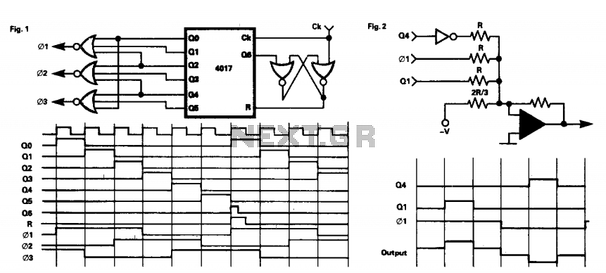
This circuit provides a three-phase square-wave output suitable for a variable speed motor drive. The operation is simple, as the 4017 counter is synchronously reset after six clock pulses. The outputs are combined to produce the necessary waveforms. It...
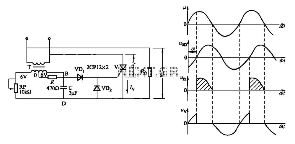
By adjusting the potentiometer RP, the output voltage of the phase shift bridge diagonal changes accordingly, which in turn alters the rectifier load power Rfz. Waveforms at respective points in FIG. 16-1 (b) illustrate this. Resistor R serves as...
The circuit serves as a foundational design, requiring experimentation for specific applications. In popular microwave bands, local oscillators (LOs) are typically generated using overtone crystal oscillators followed by multipliers. A table presents the standard LO frequencies for narrowband segments,...
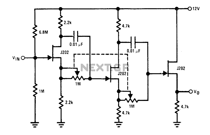
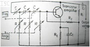
Each J202 JFET stage provides up to 180 degrees of phase shift controlled by a 1 megohm potentiometer. The potentiometer allows for complete control of the groups. JFETs are ideal for the designated circuit because they do not load...
The TBA120U is an intermediate frequency (IF) amplifier that includes a symmetrical frequency modulation (FM) demodulator and an audio frequency (AF) amplifier with adjustable output voltage. The AF amplifier features an output for volume control and an input for...