
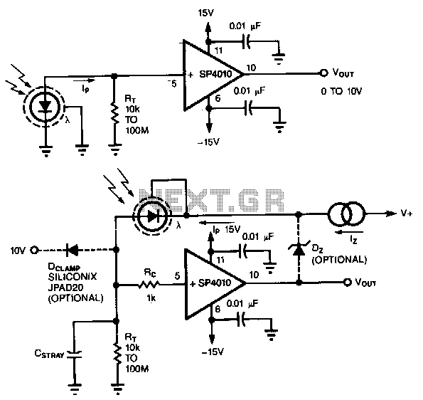
Photodiode signal conditioner

The 0.033 µF value at A3's compensation pins offers effective loop damping when the circuit is constructed using the transistors from the array in the specified configuration. The compact size of the array die results in a rapid and clean response, with a full-scale step requiring only 250 ms to stabilize at the final value. To initiate the use of this circuit, the thermal control loop must first be set. This involves grounding the base of Q3 and adjusting the 2 kΩ potentiometer so that A3's negative input voltage is 55 mV higher than its positive input. This adjustment establishes the servo's setpoint at approximately 50°C (25°C ambient + (2.2 mV/°C × 25°C rise = 55 mV = 50°C)). After ungrounding Q3's base, the array will reach the desired temperature. Subsequently, the photodiode should be placed in a completely dark environment, and the "dark trim" should be adjusted until A2's output reads 0 V. Finally, by applying or electrically simulating 1 mW of light, the "full-scale" trim can be set for a 10 V output. Once calibrated, this circuit will respond logarithmically to light inputs ranging from 10 nW to 1 mW, with accuracy limited by the diode's 1% error.
The circuit design effectively integrates the logarithmic response characteristics of the photodiode with the necessary signal conditioning elements to facilitate accurate light measurement across a wide dynamic range. The use of the CA3096 monolithic array not only simplifies the design but also enhances thermal stability and response time due to the close thermal coupling of the components. The logarithmic conversion ensures that the output voltage is proportional to the logarithm of the light intensity, allowing for a more manageable digital representation of varying light levels. The temperature control loop is critical for maintaining consistent performance, particularly in environments where temperature fluctuations may affect the characteristics of the photodiode and operational amplifiers. The careful calibration process outlined ensures that the system operates optimally, providing reliable measurements across the specified range.The photodiode specified responds linearly to light intensity over a 100 dB range. Digitizing the diodes linearly amplified output would require an A-D converter with 17 bits of range. This requirement can be eliminated by logarithmically compressing the diode's output in the signal conditioning circuity.
Al and Q4 convert the diode's photocurrent to voltage output with a logarithmic transfer function. A2 provides offsetting and additional gain. A3 and its associated components form a temperature control loop which maintains Q4 at constant temperature (all transistors in this circuit are part of a CA3096 monolithic array). The 0.033 µ¥ value at A3's compensation pins gives good loop damping if the circuit is built using the array's transistors in the location shown. Because of the array die's small size, response is quick and clean. A full-scale step requires only 250 ms to settle to final value. To use this circuit, first set the thermal control loop. To do this, ground Q3's base and set the 2 k pot so A3's negative input voltage is 55 mV above its positive input.
This places the servo's setpoint at about 50°C (25°C ambient + (2.2 mV/°C 25°C rise = 55 mV = 50°C). Unground Q3's base and the array will come to temperature. Next, place the photodiode in a completely dark environment and adjust the "dark trim" so A2's output is 0 V.
Finally, apply or electrically simulate 1 mW of light and set the ''full-scale" trim for 10 V out. Once adjusted, this circuit responds logarithmically to light inputs from lOnW to ImW with an accuracy limited by the diode's 1% error.
Related Circuits
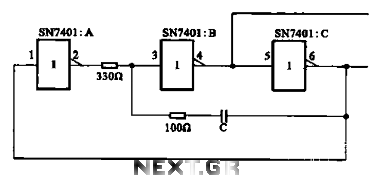
The clock signal generating circuit utilizes an RC configuration, commonly applicable in most TTL systems. This circuit requires a set of six inverters, specifically three inverters from the SN7401 series. The clock frequency is determined by the values of...
The safety shutdown and fault isolation protocol is critical in various telecommunication, industrial, and data processing systems. It is essential for data sharing. The safety shutdown and fault isolation protocol serves as a fundamental component in ensuring the reliability and...
A common method of transforming the output current of a photodiode into a voltage signal involves paralleling the photodiode with a high-value load resistor, which results in a nonlinear response. Additionally, the combination of the load's transresistance, Rr, and...
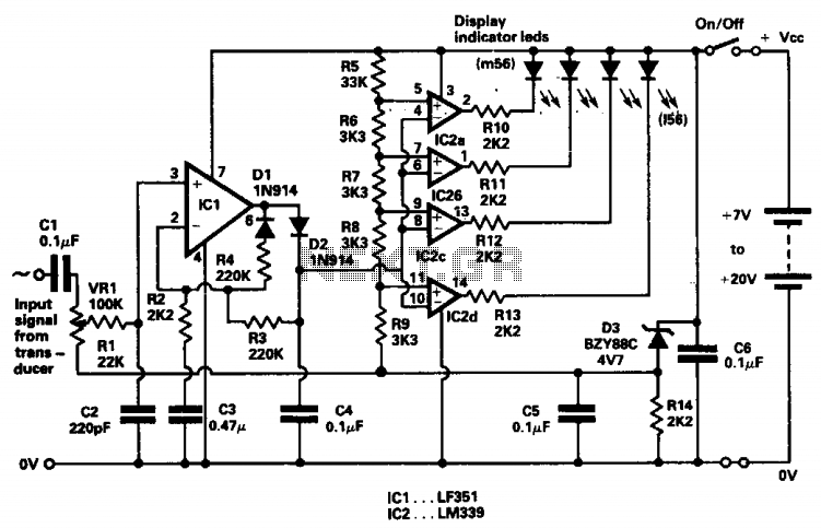
The indicator was designed to display the peak level of small AC signals from various transducers, including microphones, strain gauges, and photodiodes. The circuit responds to input signals within the audio frequency spectrum, specifically from 30 Hz to 20...
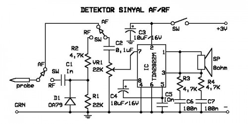
A signal detector circuit designed for detecting signals in both audio frequency (AF) and radio frequency (RF) ranges. This series is compact and straightforward to construct. The signal detector circuit operates by utilizing a combination of components such as diodes,...
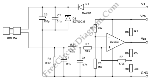
A modulated current is supplied by the integrated rotational speed sensor KMI 15/x. This current signal needs to be converted into a ground-referenced voltage signal. The KMI 15/x sensor operates by generating a modulated current proportional to the rotational speed of...