
Precision solid state time delay circuit
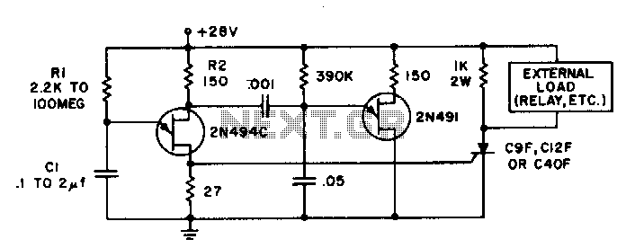
The described circuit utilizes a timing mechanism that is highly versatile, allowing for precise control of time delays without the complications associated with traditional capacitor-based timing circuits. The absence of tantalum or electrolytic capacitors enhances the reliability and longevity of the circuit, making it suitable for various applications where extended operational life is critical.
The timing function is achieved through the integration of resistor R1 and capacitor C1, which form an RC timing network. The time constant, τ (tau), of this network is calculated as τ = R1 × C1, where R1 is the resistance in ohms and C1 is the capacitance in farads. The time delay is directly proportional to this time constant, allowing for easy adjustments by varying R1 or C1.
Once the timing interval has elapsed, the 2N494C, a type of controlled rectifier, is activated. This device is designed to handle significant load currents, making it suitable for applications requiring high power. The controlled rectifier operates by switching on when a gate signal is applied, allowing current to flow through the load. The load voltage, which is the supply voltage minus approximately one volt, ensures that the load receives sufficient power for operation.
Furthermore, the option to replace R1 with a calibrated potentiometer introduces flexibility in the circuit design. By adjusting the potentiometer, the user can set a specific time delay, which is particularly useful in applications where precise timing is essential. After the initial calibration, the potentiometer can be adjusted to achieve the desired delay without the need for extensive recalibration of the entire circuit.
Overall, this circuit design provides a robust solution for applications requiring customizable time delays while maintaining high reliability and performance.Time delays from 0 milliseconds to over three minutes are possible with this circuit without using a tantalum or electrolytic capacitor. The timing interval is initiated by applying power to the circuit. At the end of the timing interval, which is determined by the value of R1C1, the 2N494C fires the controlled rectifier.
This places the supply voltage minus about one volt across the load Load currents are limited only by the rating of the controlled rectifier which is from 1 ampere up to 25 amperes for the types specified in the circuit. A calibrated potentiometer could be used in place of Rl to permit setting a predetermined time delay after one initial calibration.
🔗 External reference
Related Circuits
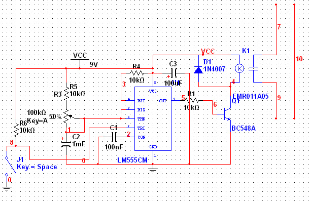
The 555 Timer has extensive applications in electronics. This document describes the use of the 555 Timer in a monostable multivibrator configuration to trigger a transistor driver that energizes a relay, which in turn operates a 230V AC lamp...
A PoE Plus power level of 30 W can be achieved by utilizing an external MOSFET along with a controller that is compatible with the older standard. Power over Ethernet (PoE) technology enables the delivery of electrical power along with...
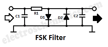
Frequency-Shift Keying (FSK) is a type of frequency modulation where the modulating signal alters the output frequency between specific predetermined values. When issues occur during the demodulation of FSK signals, utilizing an FSK filter circuit can be beneficial. Frequency-Shift Keying...
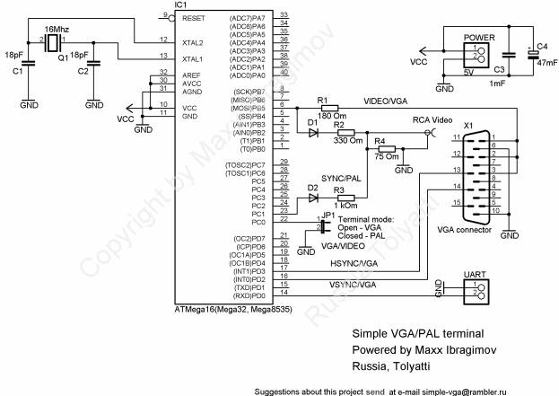
To prevent image distortion when receiving data via UART for VGA, it is advisable to conduct data exchange with the terminal approximately 300-600 microseconds after the vertical synchronization (VSYNC) signal. In a VGA system, the synchronization signals are crucial for...
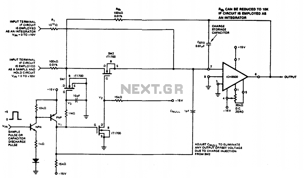
This circuit quickly charges capacitor CST0 to a voltage that matches an input signal. After charging, the input signal is electrically disconnected from the capacitor, allowing the charge to remain on CST0. Since CST0 is part of the negative...
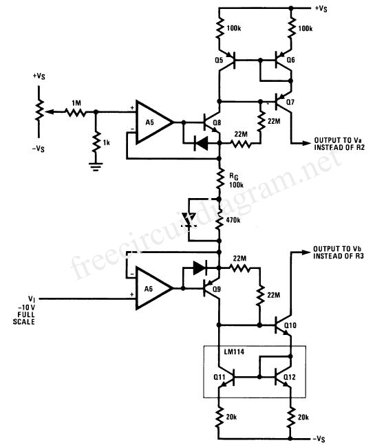
The wide-range current pump for the precision phase-locked loop (PLL) circuit is a semi-precision circuit that provides an output current proportional to -V1, with a variation of approximately 10 to 15%, across a three-decade range. The 22 MΩ resistors...