
Programmable voltage controlled timer
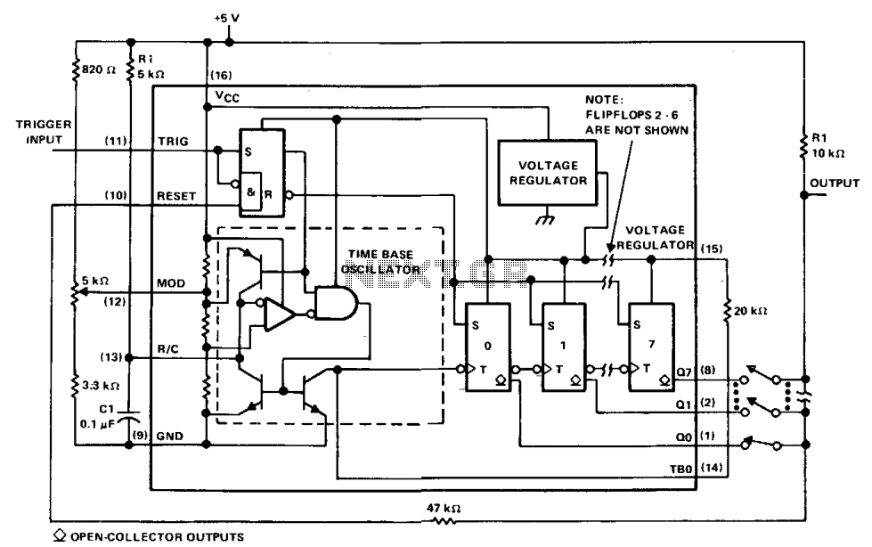
The µA2240 integrated circuit is designed to function as a versatile programmable timer, leveraging its internal architecture to deliver precise timing functions with minimal component requirements. The key feature of this device is its modulation input, which facilitates external control over the timing characteristics. By connecting a variable voltage from a potentiometer, users can dynamically adjust the input threshold, allowing for flexible timing applications.
The time base output (TBO) is a critical component of the µA2240's functionality. It operates in an open-collector configuration, which allows for easy interfacing with other digital circuits. The inclusion of a 10 kΩ pull-up resistor ensures that the output can be reliably pulled high when not actively driven low by the TBO. This configuration not only enhances signal integrity but also enables the TBO to drive subsequent logic stages, such as the 8-stage counter, effectively expanding the timer's capabilities.
Upon receiving a positive trigger pulse at startup, the TBO initiates its timing cycle, resetting all counter outputs to a low state. The open-collector nature of the counter outputs allows for a "wired-OR" logic configuration, where multiple outputs can be combined to generate a single output signal. This feature is particularly useful in applications requiring multiple timing conditions to be monitored simultaneously.
The µA2240's architecture supports the generation of up to 255 discrete time delays, each corresponding to integer multiples of the time-base period. This is accomplished by summing the binary outputs of the counter, providing a flexible method for achieving various timing requirements. The range of delays, from 200 µs to 0.223 s, makes the µA2240 suitable for a wide range of timing applications in both consumer and industrial electronics. Overall, the µA2240 presents a robust solution for programmable timing needs, combining ease of use with extensive functionality.The µA2240 may easily be configured as a programmable voltage controlled timer with a minimum number of external components. The modulation input (pin 12), which allows external adjustment of the input threshold level. A variable voltage is applied from the arm of a 10 k ohm potentiometer connected from Vcc to ground. A change in the modulation input voltage will result in a change in the time base oscillator frequency and the period of the time base output (TBO).
The TBO has an open-collector output that is connected to the regulator output via a 10 k ohm pull-up resistor. The output of the TBO drives the input to the 8-stage counter section. At start-up, a positive trigger pulse starts the TBO and sets all counter outputs to a low state. The binary outputs are open-collector stages that may be connected together to the 10 k ohm pull-up resistor to provide a "wired-OR" output function. This circuit may be used to generate 255 discrete time delays that are integer multiples of the time-base period.
The total delay is the sum of the number of time-base periods, which is the binary sum of the Q outputs connected. Delays from 200 µß to 0.223 s are possible with this configuration. 🔗 External reference
Related Circuits
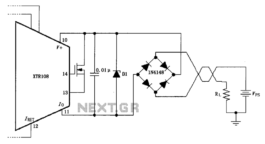
The circuit utilizes a Zener diode (D1) for overvoltage protection and a diode rectifier bridge for reverse voltage protection. The 1.4V drop across the diodes will result in a maximum voltage loss, meaning that the supply voltage (VPS) must...
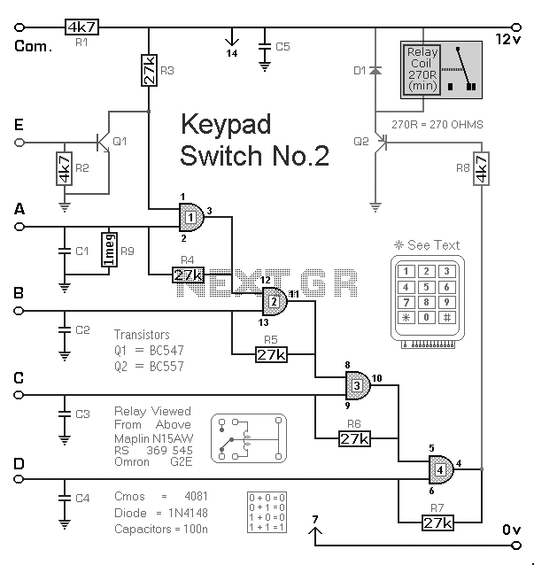
The Keypad Controlled Switch No2 Circuit operates with a 12-volt supply but is compatible with voltages ranging from 5 to 15 volts. The only requirement is to select a relay that matches the desired supply voltage. The Keypad Controlled Switch...
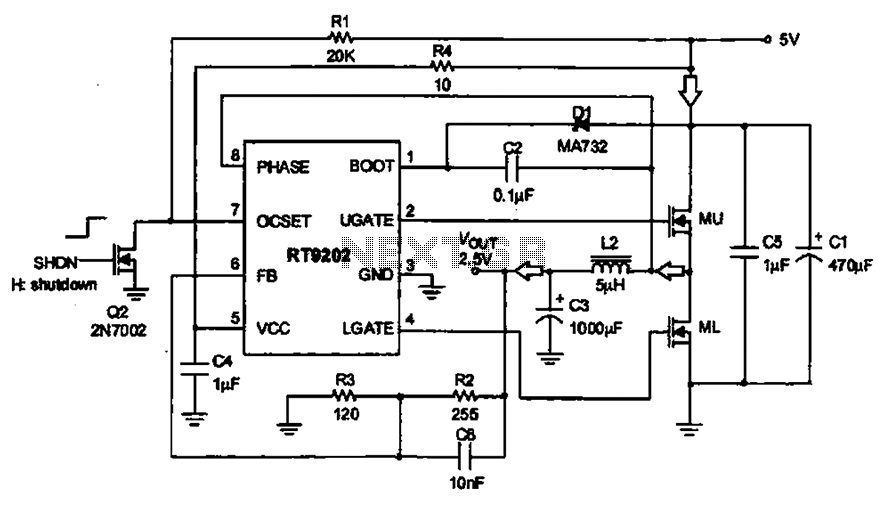
A 5V to 2.5V voltage regulator circuit is designed for use in computer motherboards. At its core, this circuit utilizes the RT9202 power management chip. The RT9202 functions as a switching pulse generating circuit, which, upon startup, converts a...

This regulator circuit can be used on an alternator that has one field terminal grounded. When the input voltage becomes too high, Q1 conducts, and the base of Q2 is driven toward ground, reducing the voltage fed to Q3....
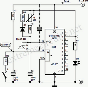
In this circuit, a 4017 CMOS decade counter can be utilized to construct a timer circuit. The push-button S1 will discharge capacitor C1 through resistor R2. The 4017 CMOS decade counter is a versatile integrated circuit that can count from...
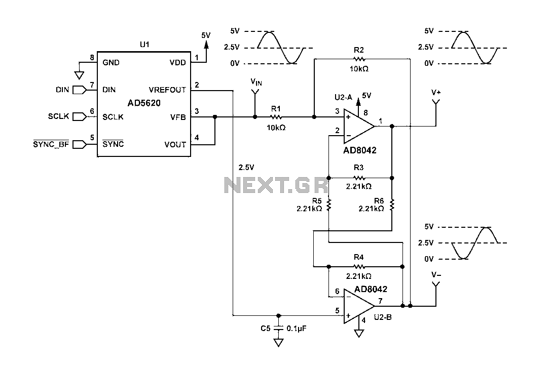
Figure 1 illustrates a circuit that utilizes a single +V power supply and a voltage output Digital-to-Analog Converter (DAC) known as the AD5620. The DAC is controlled via an SPI port, with its output ranging from 0 V to...
Warning: include(partials/cookie-banner.php): Failed to open stream: Permission denied in /var/www/html/nextgr/view-circuit.php on line 713
Warning: include(): Failed opening 'partials/cookie-banner.php' for inclusion (include_path='.:/usr/share/php') in /var/www/html/nextgr/view-circuit.php on line 713