
Pulse Frequency Modulator
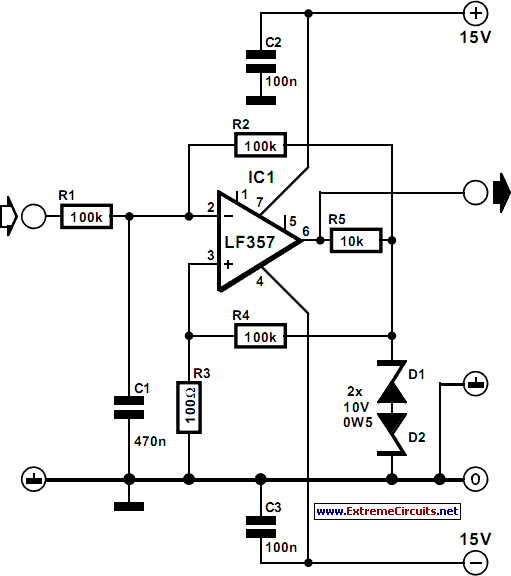
The compact pulse cum frequency modulator is designed to provide precise control over pulse width and frequency through a simple voltage-controlled mechanism. The core of the circuit is comparator IC1, which serves as the primary control element. The adjustment of the switch-over point via resistor R1 allows for modulation of the pulse width, effectively enabling the user to tailor the output characteristics to specific requirements.
The hysteresis, defined by resistors R3 and R4, plays a critical role in stabilizing the output against noise and fluctuations in the control voltage. This feature ensures that the modulator operates reliably across varying conditions. The relationship between the control voltage and frequency is crucial; at 0 V input, the maximum frequency of approximately 3.8 kHz is achieved, providing a baseline for modulation applications.
The output voltage levels of ±12 to ±13 V indicate that the modulator can interface with a range of electronic components, making it versatile for various applications. The interaction between the control voltage and the capacitor C1 determines the activation threshold of IC1, which in turn governs the timing characteristics of the output signal.
The maximum period of 25 ms represents the longest interval achievable, allowing for low-frequency applications. Adjusting the capacitance of C1 directly influences both the maximum period and the frequency output, providing flexibility in design. The inverse relationship between duty cycle and control voltage underscores the importance of careful voltage management to achieve desired output characteristics.
The minimum pulse width of approximately 6 µs at the lowest frequency indicates the modulator's ability to produce short pulses, which can be essential for high-speed applications. With a current consumption not exceeding 5 mA, the modulator is also energy-efficient, making it suitable for battery-operated devices or low-power applications. Overall, this circuit design offers a robust solution for generating modulated pulse signals across a wide range of frequencies and pulse widths.The pulse width of the compact pulse cum frequency modulator can be varied by altering the change-over point of comparator IC1 with a control voltage via resistor R1. The hysteresis of the IC is determined by resistors R3 and R4. The control voltage also causes the frequency of the present circuit to be altered. When the input voltage is 0 V, the frequency is a maximum: in the present design this is about 3. 8 kHz. The level of the output voltage is ±12 13V. The more the change-over point has been shifted with the control voltage, the longer it will take before the potential across capacitor C1 has reached the level at which IC1 is enabled. When the control voltage is larger than the zener voltage, the oscillator ceases to work. The maximum period is 25 ms, which may be adapted by altering the value of C1. This will, of course, also alter the maximum frequency. The duty cycle is inversely proportional to the control voltage. The minimum pulse width attainable at the lowest frequency is about 6 µs. The modulator draws a current not exceeding 5mA. 🔗 External reference
Related Circuits
The circuit generates a controlled pulse signal. When a high pulse signal is applied to the input terminal O (start), the output pulse signal is activated. Conversely, when a low signal is received at the input terminal O (stop),...
Mains frequency is pretty stable and it is unlikely that you have to measure it but if you have an emergency generator you might find this circuit useful as it will give an indication whether the generator is running...
This circuit provides a linear frequency increase of 10 Hz per °C over a temperature range of 0 to 100 °C and can be utilized with logic systems, including microprocessors. The temperature probe Q1, utilizing the Vbe characteristic, changes...
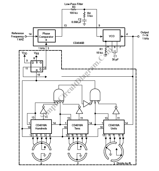
A frequency-selective frequency multiplier can be constructed using a Phase-Locked Loop (PLL) system by inserting a frequency divider within the feedback loop between the phase detector. A frequency-selective frequency multiplier utilizing a Phase-Locked Loop (PLL) system operates by manipulating the...
The advantages of synchronous reception of AM signals are well recognized, including high selectivity, linearity of detection, and a lower noise level at the output compared to other reception methods. The circuit diagram is illustrated in Figure 1. The...
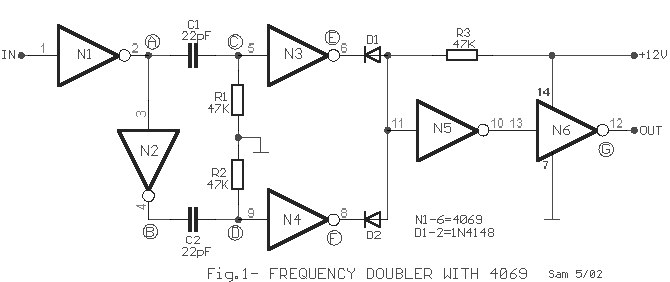
A frequency doubler can be constructed using a single 4069 hex inverter IC, resulting in an output pulse train with a frequency that is twice that of the square wave input signal. The frequency doubler circuit utilizing the 4069 hex...