
PWM Modulator
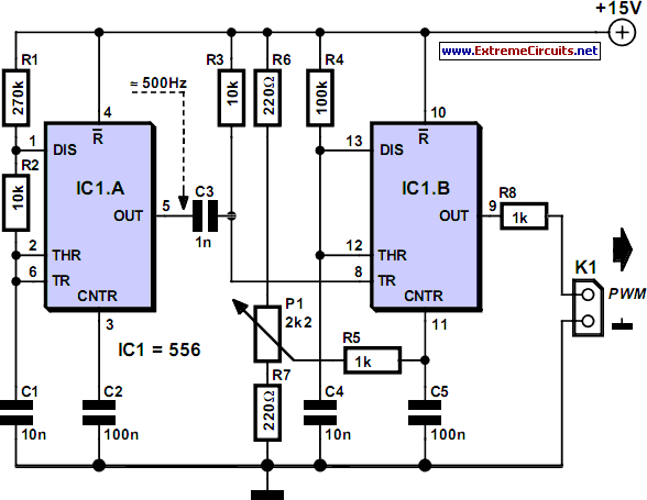
The circuit's design employs two 555 timers, one configured as an astable multivibrator and the other as a monostable multivibrator. The astable timer generates a continuous square wave at 500 Hz, with the frequency adjustable through the resistors R1 and R2, and capacitor C1. The configuration allows for a low-frequency output, minimizing electromagnetic interference during operation, which is critical in applications where signal integrity is paramount.
The monostable timer is activated by a differentiator circuit composed of R3 and C3, which ensures that the timer is triggered by a rising edge, establishing a pulse-width modulation effect. The pulse width is adjustable via potentiometer P1, allowing for fine control over the duty cycle by altering the voltage at the CNTR input. This feature enhances the versatility of the circuit, making it suitable for various dimming applications.
The output stage includes R8, which is a protective resistor that safeguards the circuit against potential short circuits, ensuring reliability and longevity. The design also incorporates a voltage regulation aspect, as the supply voltage impacts the overall control range. By utilizing a 15V supply, the circuit maintains optimal performance, with the output becoming active only when the control voltage exceeds a specified threshold.
In summary, this pulse-width modulation circuit offers a simple yet effective solution for controlling the brightness of lamps or other loads through a well-designed dual 555 timer configuration. The careful selection of components and the inclusion of protective features make it a robust choice for experimentation and practical applications in electronic dimming solutions.If you ever thought of experimenting with pulse-width modulation, this circuit should get you started nicely. We`ve kept simplicity in mind and used a dual 555 timer, making the circuit a piece of cake. We have even designed a small PCB for this, so building it shouldn`t be a problem at all. This certainly isn`t an original circuit, and is here ma inly as an addition to the Dimmer with MOSFET` article elsewhere in this website. The design has therefore been tailored to this use. A frequency of 500 Hz was chosen, splitting each half-period of the dimmer into five (a low frequency generates less interference). The first timer is configured as a standard astable frequency generator. There is no need to explain its operation here, since this can easily be found on the Internet in the datasheet and application notes.
All we need to mention is that the frequency equals 1. 49 / (R1+2R2) G— C1) [Hz] R2 has been kept small so that the frequency can be varied easily by adjusting the values of R1 and/or C1. The second timer works as a monostable multivibrator and is triggered by the differentiator constructed using R3 and C3.
The trigger input reacts to a rising edge. A low level at the trigger input forces the output of the timer low. R3 and C3 have therefore been added, to make the control range as large as possible. The pulse-width of the monostable timer is given by 1. 1xR4xC4 and in this case equals just over a millisecond. This is roughly half the period of IC1a. The pulse-width is varied using P1 to change the voltage on the CNTR input. This changes the voltage to the internal comparators of the timer and hence varies the time required to charge up C4. The control range is also affected by the supply voltage; hence we`ve chosen 15V for this. The voltage range of P1 is limited by R6, R7 and R5. In this design the control voltage varies between 3. 32 V and 12. 55 V (the supply voltage of the prototype was 14. 8 V). Only when the voltage reaches 3. 51 V does the output become active, with a duty-cycle of 13. 5 %. The advantage of this initial quiet` range is that the lamp will be off. R8 protects the output against short circuits. With the opto-coupler of the dimmer as load, the maximum current consumption of the circuit is about 30 mA.
🔗 External reference
Related Circuits
A commercial motor controller is more than just a circuit designed to adjust the speed of a motor. It encompasses various features that enhance its functionality, which are explained in a guided overview. To effectively control the speed of...

The PWM controller utilizes complementary half-H peripheral drivers SN75603 and SN75604, featuring totem-pole outputs rated at 40 V and 2.0 A. These drivers effectively configure the motor in a full-bridge setup, enabling bidirectional control. Timer U1 operates in astable...
The FM oscillator/modulator is a voltage-controlled oscillator that demonstrates a nearly linear relationship between output frequency and input voltage across a broad frequency deviation. It serves as an effective FM source with minimal additional components required. The device operates...
This FSK demodulator converts the FSK signal into a serial digital signal. FSK modulation is employed to transmit digital serial data, and demodulation is necessary to retrieve this data. The FSK (Frequency Shift Keying) demodulator is a crucial component in...

As the number of stations increased and the power levels also rose, receiver performance had to be enhanced. The pentagrid converter, such as the 6BE6 tube (British EK90 valve), was introduced, which was optimized for mixer performance. This included...
A 2N3904 in the base circuit sets the Q point of the amplifier. FM subcarrier audio at 4.5 MHz is also injected at this point through a 3300 ohm resistor and a DC blocking capacitor. A high frequency 5-watt...
Warning: include(partials/cookie-banner.php): Failed to open stream: Permission denied in /var/www/html/nextgr/view-circuit.php on line 713
Warning: include(): Failed opening 'partials/cookie-banner.php' for inclusion (include_path='.:/usr/share/php') in /var/www/html/nextgr/view-circuit.php on line 713