
PWM - Pulse Width Modulation for DC Motor Speed and LED Brightness 2

The 74AC14 PWM circuit operates on the principle of pulse-width modulation (PWM) to control the power supplied to a load. The components involved include a capacitor (C2), a potentiometer (R2), and two diodes (D1 and D2) arranged in a configuration that influences the charging and discharging cycles of the capacitor. The inverter gate plays a critical role in determining the state of the output based on the voltage across the capacitor.
When power is initially applied, the capacitor (C2) is in a discharged state, resulting in a low input to the inverter gate. This low input causes the inverter to output a high signal, allowing current to flow through R2 and D1, charging the capacitor. The charging time is adjustable via the potentiometer; a lower resistance allows for a quicker charge, while a higher resistance slows the charge process.
Once charged, the inverter gate's output transitions to low, causing the capacitor to discharge through D2 and the right side of the potentiometer. The discharge time is also influenced by the potentiometer setting, allowing for fine-tuning of the duty cycle. The diodes ensure that current flows in one direction, creating an asymmetrical charging and discharging cycle that is essential for PWM functionality.
This arrangement enables the circuit to produce a variable duty cycle, which is critical for applications such as motor speed control, LED brightness modulation, and other scenarios where varying power levels are required. The ability to adjust the duty cycle from near 0% to 100% allows for precise control over the output power delivered to the load, making this circuit versatile and widely applicable in various electronic applications.To understand how the 74AC14 PWM circuit works, let`s zoom in on the section of the schematic containing the trimpot, diodes, capacitor, and the first inverter logic gate. The capacitor is empty (discharged) when the power is first applied to the circuit. Because the capacitor is low, and because the capacitor is connected to the input pin of the inverter gate, the input is low. The conventional current flows from the output of the inverter gate through the left half of the potentiometer (R2) and then through diode D1. The current cannot flow through the right half of the variable resistor (R2) because diode D2 blocks the path (notice the direction of the diode arrow).
Diodes are one-way valves. The current flows into the capacitor (C2); charging the capacitor. If the potentiometer is dialed to the far left, the resistance will be small and the capacitor will charge quickly. If the potentiometer is dialed to the far right, the resistance will be large and the capacitor will charge slowly.
Eventually, the capacitor fills up (is charged). Because the capacitor is now high, and because the capacitor is connected to the input pin of the inverter gate, the input is now high. The conventional current flows from the capacitor (C2), through diode D2, and then through the right half of the potentiometer (R2).
If the potentiometer is dialed to the far right, the resistance will be small and the capacitor will discharge quickly. If the potentiometer is dialed to the far left, the resistance will be large and the capacitor will charge slowly.
The repeated charging and discharging of the capacitor occurs because the inverter gate output flips to the opposite of the state of the capacitor. When the capacitor is empty, the inverter output charges the capacitor. When the capacitor is full, the inverter output discharges the capacitor. If this were the only feature of this circuit, the output would be on half of the time (when charging the capacitor) and off half of the time.
This would provide 50% power (only on half the time) to whatever was connected. The trick is that the resistance of the on path is different from the off path due to the diodes. That means you can dial the trimpot to make the on time take more or less time than the off time .
As such, you can supply an output signal that is on from almost 0% to 100% of the time. Obviously if the outputs are on only 10% of the time, the attached device is only going to be on only 10% of the time. In this way, the total amount of power delivered to an attached device can be varied by simply turning the potentiometer to alter the on/off times (duty cycle).
🔗 External reference
Related Circuits
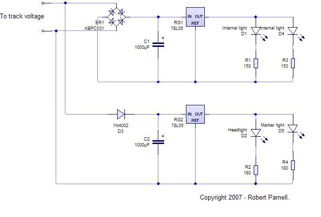
An LED, or Light Emitting Diode, is a semiconductor device that allows current to flow in one direction while blocking it in the opposite direction. This characteristic makes LEDs polarized components, having a positive side known as the anode...
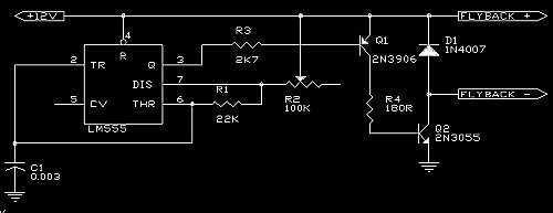
A 555 is used as an oscillator, optimally around 15.76KHz (in North America). Power pins on the chip (pin 1 to ground, pin 8 to +12V) are not shown on the diagram. The output from the 555 is then...
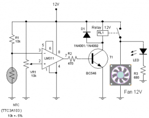
The circuit schematic diagram of a fan speed control system that activates only when necessary. When the transistor heats up, the fan will automatically turn on. The fan speed control circuit operates based on the temperature of the transistor, utilizing...
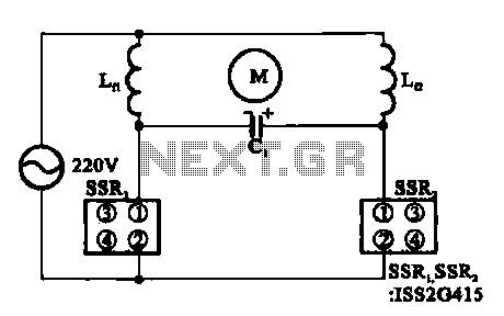
The triac motor drive circuit depicted demonstrates the operation of a TRIAC, which is often referred to as a solid-state relay. Figure (a) illustrates the circuit configuration, while figure (b) presents the connections for the motor coils. The triac motor...
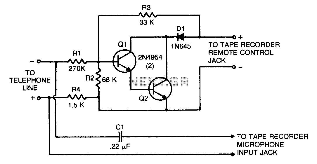
This circuit transforms a tape recorder into a fully automatic device for recording telephone conversations without requiring an external power source. The voltage at the switch terminals of the tape recorder is applied to a pair of Darlington-connected transistors,...
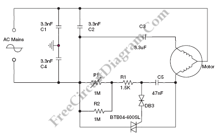
This circuit diagram can be utilized to adjust the speed of a low-power induction motor, commonly found in fan applications. The circuit for controlling the speed of a low-power induction motor typically employs a variable frequency drive (VFD) or a...