
Regulated Charge Pump

The described DC-DC converter circuit operates by utilizing a voltage tripler configuration that eliminates the need for an external inductor and diode, which are commonly found in traditional switching regulators. The core of this design involves an integrated circuit, IC1, which features a built-in 50 kHz oscillator responsible for generating the EXT signal at pin 6. This signal serves as the primary control input for the MOSFET driver, IC2.
IC2 contains both inverting and non-inverting amplifiers that facilitate the generation of drive signals that are 180° out of phase. This phase difference is crucial for the effective operation of the diode-capacitor tripling network, which consists of diodes D1, D2, and D3, along with capacitors C1, C2, and C3. The tripling network effectively multiplies the input voltage, allowing the capacitors to charge and discharge in a coordinated manner, ultimately recharging capacitor C3 to a target voltage of approximately 10 V every 20 cycles.
To ensure a stable output voltage with minimal fluctuations, a ferrite bead is employed to limit output ripple to about 20 mVpp when a load of 50 mA is applied. This feature is essential for applications requiring a clean and stable voltage supply. The overall conversion efficiency of the circuit is around 70%, which is a practical performance level for a configuration that converts a 5 V input to a 10 V output. This efficiency is a critical factor in battery-powered applications where energy conservation is paramount.
In summary, this DC-DC converter design effectively utilizes a voltage tripler configuration to achieve a higher output voltage while maintaining efficiency and minimizing output ripple, making it suitable for various electronic applications. The dc-dc converter substitutes a voltage tripler in place of the external inductor and the diode that"s typically as sociated with the switching regulator, IC1. Inverting and noninverting amplifiers in the MOS-FET-driver (IC2) activate a diode-capacitor tripling network (D1 through D3, CI through C3). A 50-kHz oscillator residing within IC1 produces the EXT signal (pin 6), IC2 converts this signal into drive signals (180° out of phase) for the tripler.
The resulting charge-discharge action in the capacitors recharges C3 toward 10 V every 20 The ferrite bead limits output ripple to about 20-mVpp for a 50-mA load. Conversion efficiency is about 70% for the 5-V input, 10-V output configuration.
Related Circuits

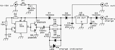
This is a simple and low-cost NiCd and NiMH battery charger. The schematic diagram indicates that the charging current (I) should be set to 1/10 of the battery's rated capacity. For instance, if the battery has a rated capacity...
A charger is essential for charging a 12 Volt battery from a 12 Volt source due to the typical voltage variation between 11 Volt and 15 Volt. A battery requires a controlled charge current and voltage, which cannot be...
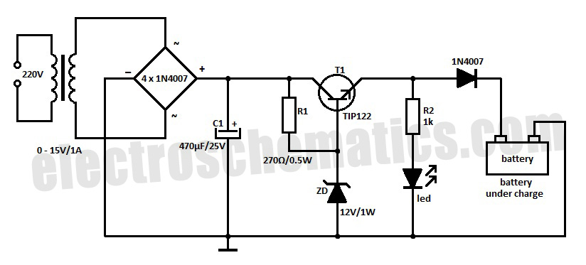
Most battery chargers lack provisions for current and voltage regulation. The step-down voltage is primarily utilized for charging purposes. Many battery chargers operate on a straightforward principle of reducing the input voltage to a level suitable for charging a battery....
The input voltage for the high-voltage DC-DC converter is 12V AC at 800mA, which is then converted to DC using a 1A bridge rectifier diode. The output voltage of the converter can be adjusted within the range of 0-1000V...
The discharge control circuit consists of a battery management system designed to prevent over-discharge of a battery. It features a relay control mechanism that activates when the battery voltage drops below a specified threshold of approximately 10.5V. The circuit...
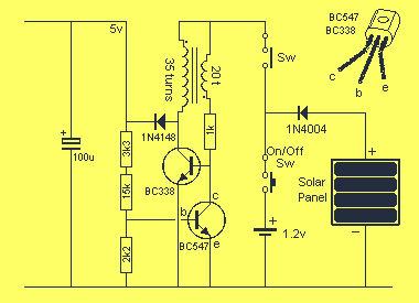
This project uses the 1.2v rechargeable battery and solar panel from a Solar Garden Light. These lights can be bought for less than $5.00 in most $2.00 shops or similar shops that sell general household items. We are also...