
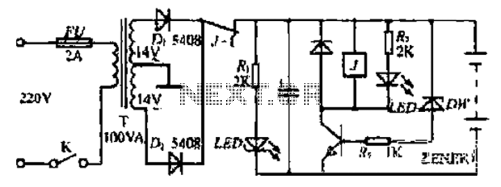
regulated dc power supply

The circuit employs a low ripple regulated DC power supply architecture that is efficient in high current applications. The use of a Darlington pair (Q1 and Q2) significantly enhances the current amplification capability. Q1 acts as the first transistor in the pair, providing initial current gain, while Q2 further amplifies this current, allowing the circuit to handle loads exceeding the limitations of standard linear regulators.
The zener diode D2 plays a crucial role in voltage regulation by maintaining a stable reference voltage. Its operation in the breakdown region ensures that fluctuations in input voltage do not affect the output voltage significantly. Resistor R1 is strategically placed to provide the necessary base current to Q1 while also ensuring that D2 remains in its active region, thus stabilizing the entire voltage regulation process.
In operation, the circuit dynamically adjusts to changes in load and input voltage. An increase in input voltage leads to an increase in output voltage, which is countered by the feedback mechanism involving Q2's base-emitter voltage. The feedback loop ensures that as the output voltage rises, the base-emitter voltage of Q2 decreases, which in turn increases its collector-emitter resistance, effectively reducing the output voltage back to the desired level. This self-regulating feature is essential for maintaining the desired output voltage under varying load conditions.
Overall, this transistor-based voltage regulator design is robust and capable of delivering a stable output voltage with minimal ripple, making it suitable for various high-current applications in electronic circuits.A low ripple regulated DC power supply designed based on transistors is shown here. Such transistor voltage regulators are suitable for application where high output current is required. Conventional integrated series regulators like 7805 can only deliver up to 1A. Additional series pass transistors have to be added to the 7805 based regulator cir cuit for improving their current capacity. The circuit shown below is a basic series voltage regulator based on transistors. Transistor Q1 (2N 3054) and Q2 (2N 3055) form a darlington pair. Resistor R1 provides the base current for Q1 and also keeps the zener diode D2 in the active region. The overall working of the circuit can be demonstrated by explaining two situations. When the input voltage (output of the rectifier section) increases, the output voltage of the regulator (Vout) also increases. This increase in Vout decreases the base emitter voltage of Q2 because the zener diode D2 is operating in the breakdown region and the voltage across it is unchangeable.
This decrease in VBEincreases the collector emitter resistance of Q2 and so the output voltage (Vout) gets reduced accordingly. When the output load increases, the output voltage (Vout) gets reduced. This decrease of output voltage (Vout) makes VBEof Q2 to decrease. This reduces the collector emitter resistance of Q2 and so the output voltage gets increased accordingly.
🔗 External reference
Related Circuits
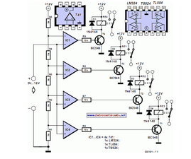
This circuit demonstrates that microprocessors, personal computers, and the latest ultra-accurate digital-to-analog converters (DACs) are excessive for the task of sequentially controlling four relays. The circuit utilizes a simple microcontroller or a basic timer IC to manage the operation of...
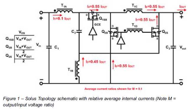
The ability to reduce power losses is crucial. This document describes a new ultra-high-performance topology that is expected to serve as the foundation for next-generation DC-DC power supplies in high-demand applications. The proposed ultra-high-performance topology aims to significantly enhance the...
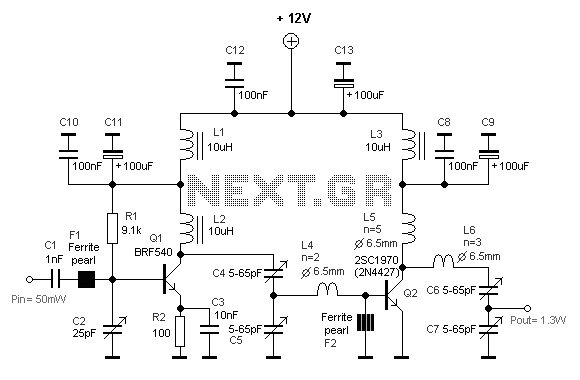
Some amplifier is based around a RF transistor. In my case I will use a common NPN RF transistor called 2SC1970. You can also use other transistors like 2N4427 and some others. Check datasheets to see how much power...
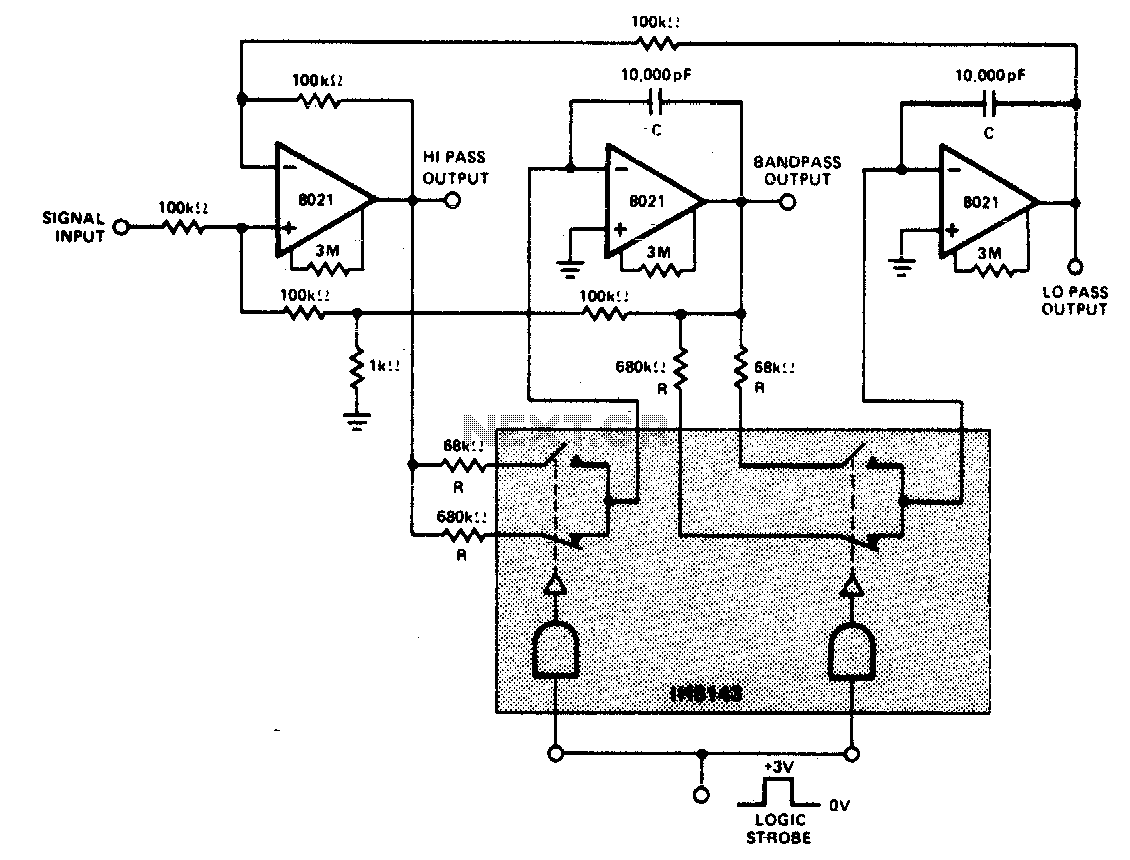
A constant gain, constant Q, variable frequency filter that provides simultaneous low-pass, bandpass, and high-pass outputs. With the specified component values, the center frequency will be 235 Hz and 23 Hz for high and low logic inputs, respectively, with...
Bidirectional control is implemented for a motor to increase its operational degree. The motor can rotate in either direction with a current of 1A. A variable duty cycle multivibrator is utilized to achieve the construction and control of the...
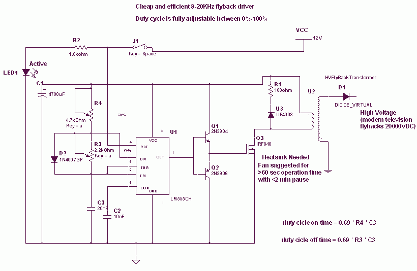
The 555 is wired as an astable and the capacitor is charged only through the 4.7Kohm trimmer (notice the diode) and discharged only through the 2.2 Kohm trimmer, making the duty cycle fully adjustable. The square wave is then...