
RF isolation amplifier
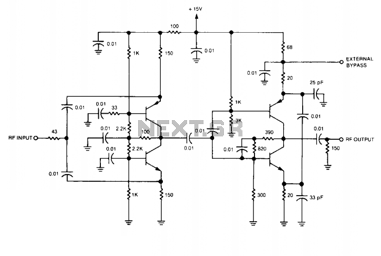
The described wideband RF isolation amplifier is engineered for applications demanding a broad frequency range and exceptional isolation between input and output stages. Operating within a frequency range of 0.5 to 400 MHz, the amplifier maintains a consistent gain variation of ± 0.5 dB, ensuring reliable performance across its operational bandwidth.
The amplifier consists of two stages, each designed to enhance the overall performance and isolation characteristics. The input stage, configured as a common-base amplifier, is particularly effective in minimizing the effect of input capacitance, thus enhancing the amplifier's ability to handle high-frequency signals with minimal distortion. This configuration allows for a lower input impedance, which is advantageous in applications where signal sources may have limited drive capability.
The output stage employs a common-emitter configuration, which is known for providing significant voltage gain. The use of emitter degeneration in this stage serves to linearize the amplifier's response and improve its stability by reducing the gain sensitivity to variations in transistor parameters. Additionally, the incorporation of collector-base feedback enhances the amplifier's input and output impedance matching, further contributing to its overall performance.
This RF isolation amplifier is particularly suitable for integration into receiver IF strips, where high reverse isolation is crucial to prevent unwanted feedback and interference. Furthermore, it can be effectively utilized in frequency distribution systems, where maintaining signal integrity over a wide bandwidth is essential. The combination of complementary-symmetry transistor arrangements in both stages not only optimizes performance but also ensures thermal stability, making the amplifier reliable for prolonged use in demanding environments.This wideband RF isolation amplifier has a frequency response of 0.5 to 400 MHz ± 0.5 dB. This two stage amplifier can be used in applications requiring high reverse isolation, such as receiver intermediate-frequency (IF) strips and frequency distribution systems. Both stages use complementary-symmetry transistor arrangements. The input stage is a common-base connection for the complementary circuit. The output stage, which supplies the positive gain, is a common-emitter circuit using emitter degeneration and collector-base feedback for impedance control. 🔗 External reference
Related Circuits
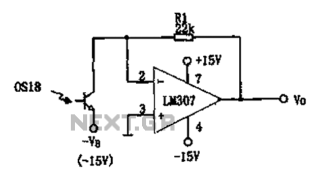
The circuit described is a photoelectric receiver amplifier designed to amplify the electrical signals generated by photodiodes or phototransistors in optoelectronic devices. When the intensity of incident light varies, the photosensitive device generates a corresponding voltage or current. The...
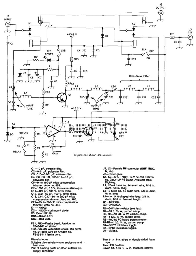
A 100 W output at 50 MHz is available from this circuit. U1 and Q2 form a T-R relay driver, switching the amplifier on when RF input at J1 is sensed. During receive periods, J1 and J2 are directly...
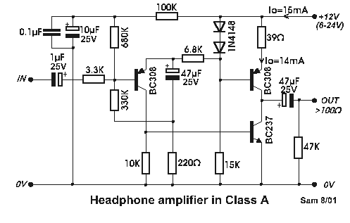
Even if simple the circuit, plirej' all condition, regarding the distortion and the response of frequency. The resistance of entry is 250K and the load that can drive is between 100R and 2K. The circuit use negative coupling. His...
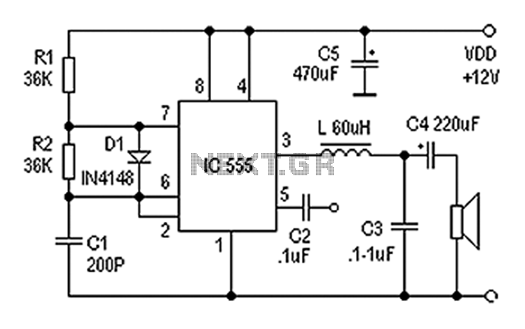
Also known as a digital amplifier, the Class-D amplifier is characterized by its compact size and high efficiency. This circuit utilizes a 555 timer IC to create a Class D amplifier. The 555 timer operates as a controllable multivibrator,...
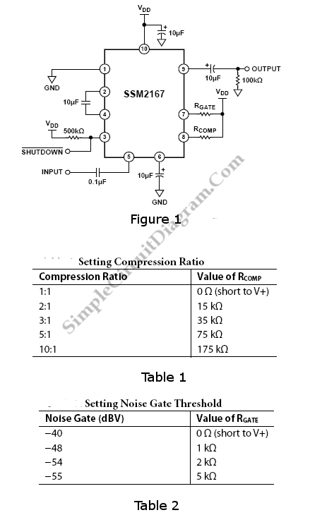
In personal electronics and computer audio systems, the SSM2167 is a complete and flexible solution for conditioning microphone inputs. It is also very good for various applications. The SSM2167 is an integrated circuit specifically designed for microphone preamplification and audio...
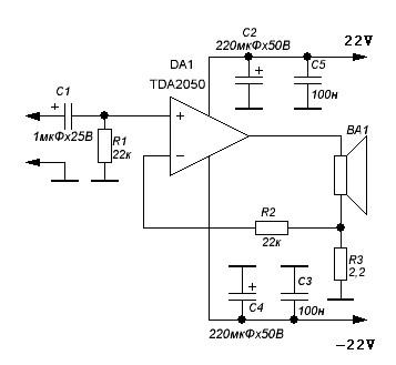
TDA2050 audio amplifier circuit diagram. The circuit incorporates environmental protection, where the output signal travels through connecting cables and the speaker’s network. In this case, the reactance of the circuit section connected to pin 4 of the chip is...