
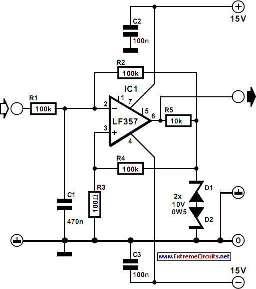
RF modulator
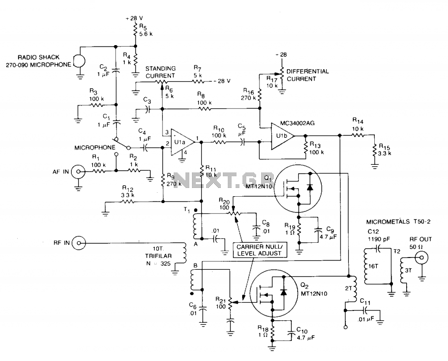
The circuit operates by utilizing transformer T1, which is critical for coupling the RF input to the field-effect transistors (FETs) Q1 and Q2. These transistors are configured to handle the RF signals effectively, ensuring that when they are driven with equal amplitude but opposite phase signals, they will cancel each other out at the output when AF modulation is absent.
The introduction of audio frequency (AF) modulation at points A and B alters the phase relationship between the signals fed to the FETs. This modulation is crucial for generating a usable RF output, as it allows for the combination of the two signals in such a way that they no longer cancel each other out, but instead produce a modulated RF signal at the output.
The inclusion of resistors R18 and R19 serves to improve the overall stability of the DC operating point of the circuit, while also enhancing the low-frequency gain. These resistors provide a feedback mechanism that stabilizes the transistors' operation, preventing distortion and ensuring that the circuit maintains its performance across varying input conditions.
The phase inverter, utilizing dual op-amps U1a and U1b, plays a significant role in producing the necessary out-of-phase AF modulation signals. This configuration allows for precise control of the modulation depth and ensures that the signals fed to the FETs are properly balanced, which is essential for the effective operation of the RF output stage.
Overall, this circuit design exemplifies a well-engineered approach to RF amplification and modulation, utilizing key components such as transformers, FETs, resistors, and op-amps to achieve a reliable and efficient output.An RF input is applied to the primary of Tl, which applies equal amplitude, opposite phase RF drive for output FETs Ql and Q2. With no AF modulation at points A and B, the opposite phase RF signals cancel each other and no output appears at the 50 V output connector.
When AF modulation is applied to points A and B, a modulated RF output is obtained. The dc stability and low frequency gain are improved by source resistors R18 and R19. A phase inverter consisting of a dual op amp (Ula and Ulb) produces the out-of-phase, equal amplitude AF modulation signals. 🔗 External reference
Related Circuits
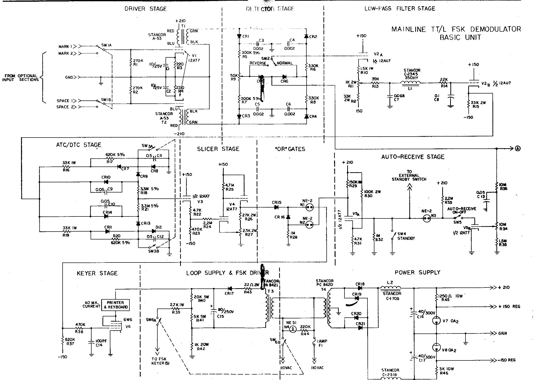
The term "demodulator" is becoming a standard in both commercial and military sectors. "Converters" are often associated with devices that automatically transform Morse code into RTTY, convert 8-level signals to 5-level, or adjust baud rates from 50 to 45,...
Although there is a need for an integrated circuit (IC), the interface between the modulator and audio-video signals has not yet been developed as an IC. This is primarily due to the complexity of such a design, the variations...

If you have considered experimenting with pulse-width modulation, this circuit serves as an excellent starting point. Simplicity has been prioritized in the design, utilizing a dual... This circuit is designed to facilitate experimentation with pulse-width modulation (PWM), a technique widely...
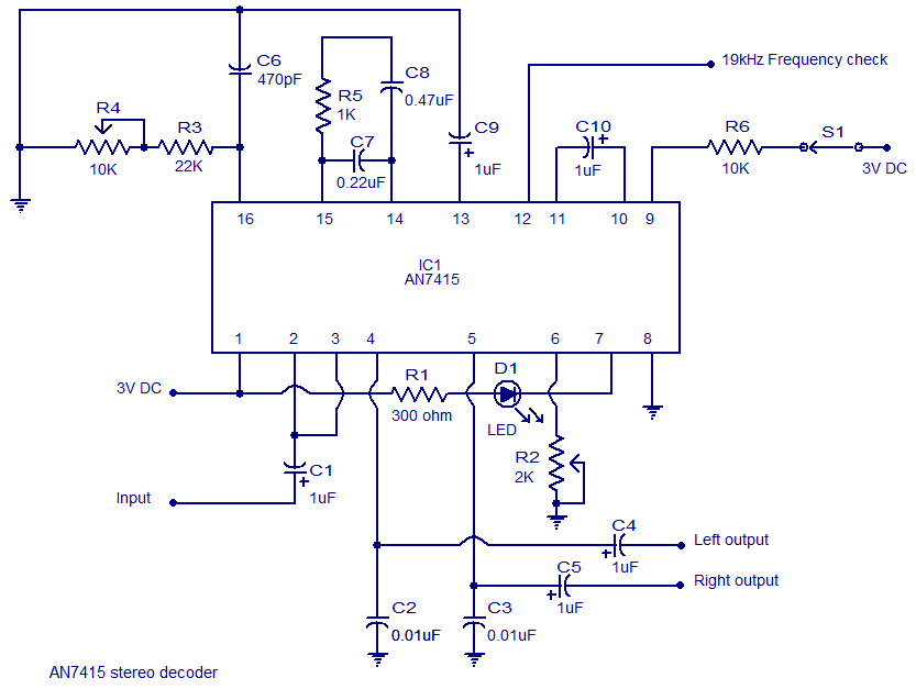
The AN7415 is a monolithic integrated circuit designed for FM stereo demodulation applications. It operates within a voltage range of 1.6 to 7 V DC, making it suitable for handheld FM radios powered by two AA dry cells. This...
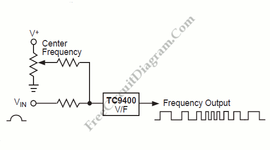
Designing various electronic circuit systems (synthesizer, modem, decoder, data converter, etc.) often requires a frequency modulator subsystem. An FM modulator is a crucial component in these systems. An FM modulator is an electronic device that encodes information in a carrier...
The pulse width of the compact pulse cum frequency modulator can be adjusted by changing the switch-over point of comparator IC1 using a control voltage through resistor R1. The hysteresis of the IC is set by resistors R3 and...