
Schematic diagram of a USB player Schematic Diagram
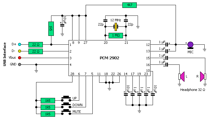
The USB circuit featuring the PCM2902 IC is designed to facilitate the conversion of digital audio signals from a USB source into analog signals suitable for audio playback. This process is essential for enabling devices such as headphones and speakers, which require analog input to function correctly.
The PCM2902 is a USB audio interface that integrates a stereo digital-to-analog converter (DAC), allowing for high-quality audio output. The circuit typically includes several key components:
1. **USB Interface**: The USB port acts as the primary input, where digital audio data is received from a computer or other USB-enabled device.
2. **PCM2902 IC**: This IC is the heart of the circuit, responsible for decoding the incoming digital audio signals. It converts the digital data into analog signals that can be sent to an audio output device.
3. **Low-Pass Filter**: After the DAC conversion, a low-pass filter may be implemented to smooth out the output signal, reducing high-frequency noise that could affect audio quality.
4. **Power Amplifier**: If the audio output is intended for speakers, a power amplifier circuit is included to boost the signal strength. This amplification ensures that the audio can be heard clearly at higher volumes.
5. **Output Connections**: The circuit features output connections for both headphones and speakers, allowing for versatile audio playback options.
The schematic diagram for this USB player circuit will typically illustrate the connections between these components, highlighting the flow of data from the USB interface through the PCM2902 and onto the output devices. Proper attention to component values and circuit layout is crucial for achieving optimal audio performance and minimizing distortion.In this usb circuit using an IC as a modifier of digital voice data into analog so that it can be applied to a headphone, or again through the power amlplifier strengthened so that it can be heard through the speakers. IC used in this circuit using IC PCM2902 as a modifier of a digital data into analog data storage. You are reading the Circuits of Schematic diagram of a USB player And this circuit permalink url it is 🔗 External reference
Related Circuits
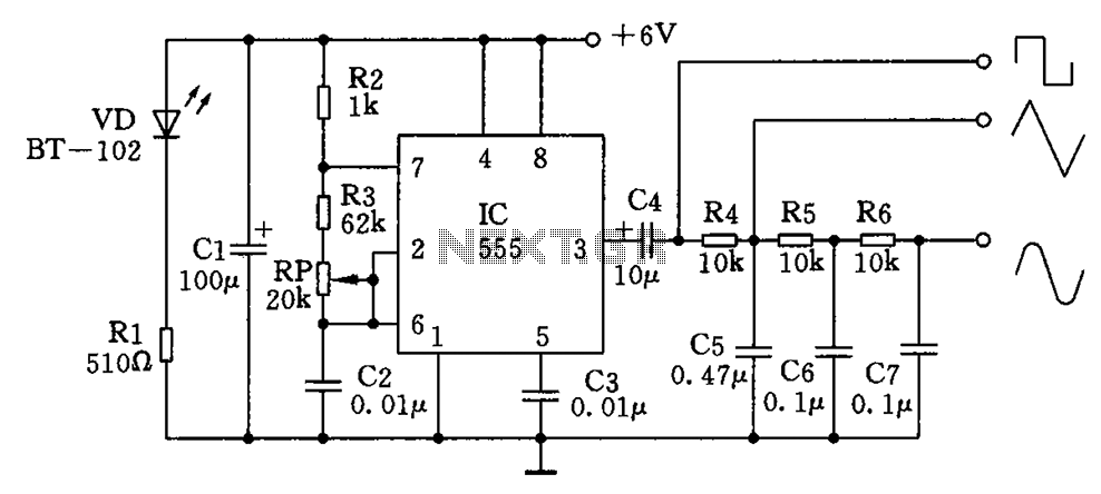
The circuit simultaneously generates a square wave, triangle wave, and sine wave, making it particularly suitable for electronics enthusiasts and students who wish to observe signal waveforms using an oscilloscope. This signal generator circuit is simple, low-cost, and allows...
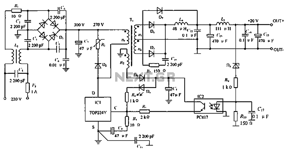
The circuit depicted in the figure is designed to achieve a higher power output by modifying specific components. On the left side of the figure, components R1, L1, D1, and capacitors C1 to C7 form a conventional filtering and...
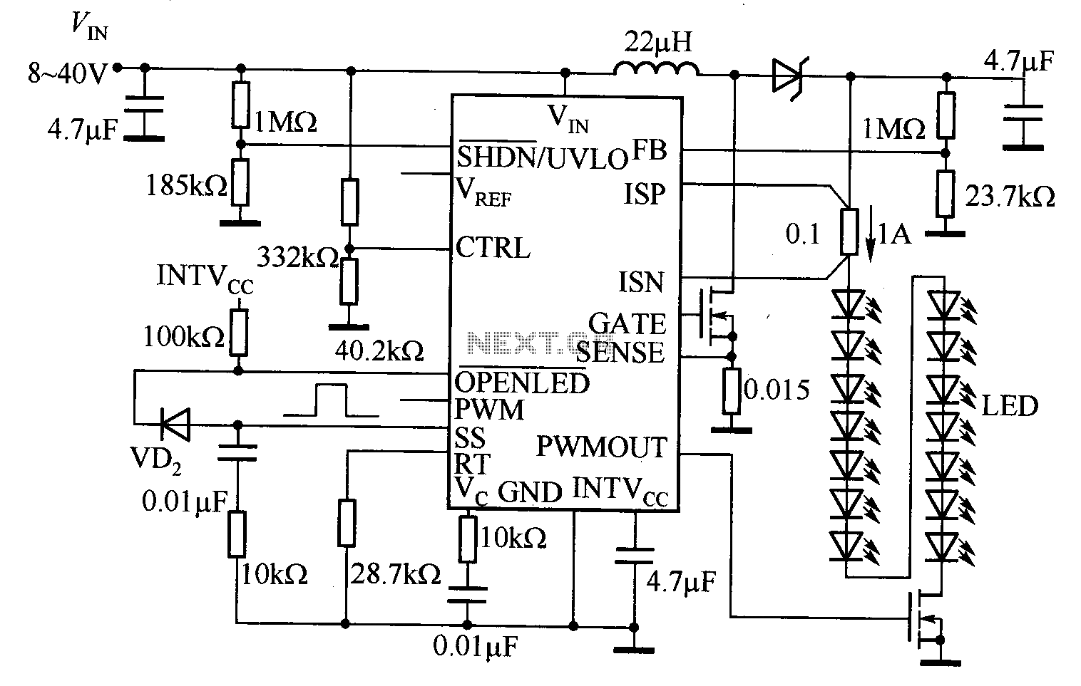
The LT3755 is utilized for high-side current sensing in LED strings, enabling flexible programming and control. It supports a PWM input that allows for a dimming ratio of up to 3000:1, while the CTRL input offers additional analog dimming...
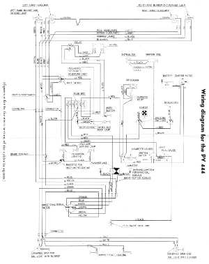
The following circuit illustrates the wiring diagram for the Volvo PV444, a vintage car electrical circuit. It provides an electrical understanding of this uni-body vehicle. The Volvo PV444 wiring diagram serves as a crucial reference for understanding the electrical system...
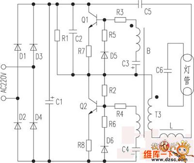
The saving lamp circuit features two main types: glass cover and exposed. The glass cover variants include three series: spherical, cylindrical, and processing types. The first two series consist of four variations: transparent, carved, engraved, and white. These lamps...
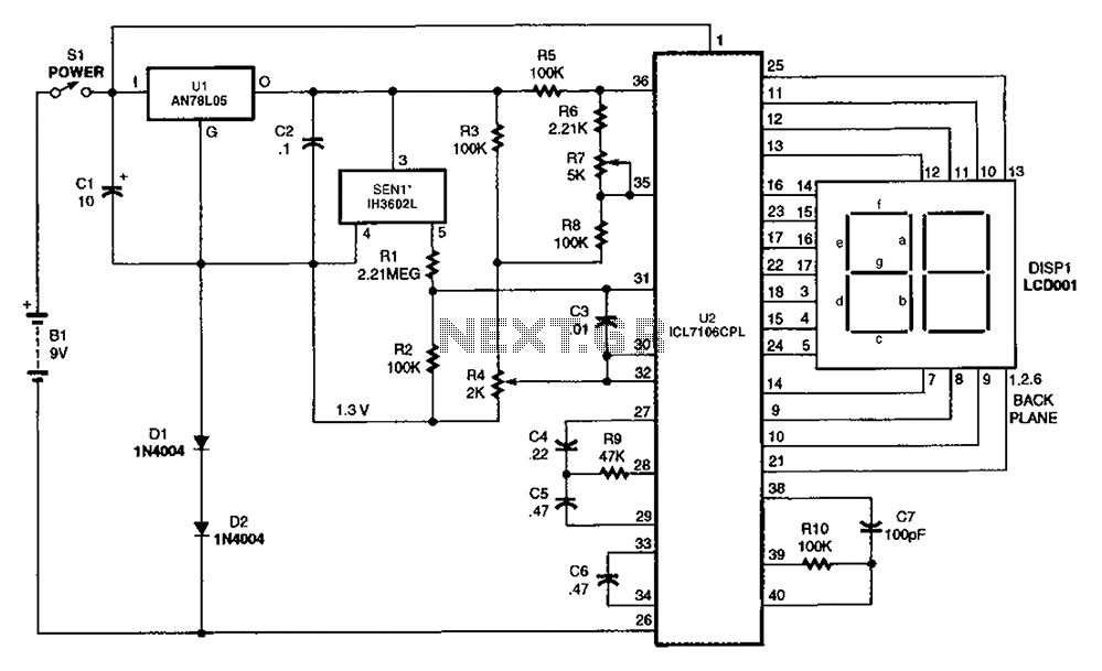
The output DC voltage of sensor SEN1 changes linearly in response to variations in relative humidity. This DC voltage is routed through resistors R1 and R2 to the analog-to-digital (A/D) converter chip U2. Resistor R4 is connected to ground,...